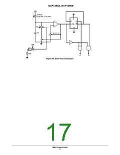
NCP1396A, NCP1396B
As described in the data-sheet, two startup levels
for the direct a connection from a 12 V source. Thanks to
this NCP1396B, simple ON/OFF operation is therefore
feasible.
VCC(on) are available, via two circuit versions. The
NCP1396 features sufficient hysteresis (3 V typically) to
allow a classical startup method with a resistor connected
to the bulk capacitor. Then, at the end of the startup
sequence, an auxiliary winding is supposed to take over the
controller supply voltage. To the opposite, for applications
where the resonant controller is powered from a standby
power supply, the startup level is 10 V typically and allows
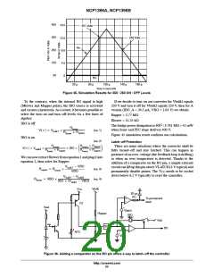
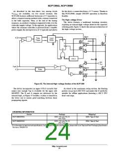
The High--voltage Driver
The driver features a traditional bootstrap circuitry,
requiring an external high-voltage diode for the capacitor
refueling path. Figure 52 shows the internal architecture of
the high-voltage section.
HV
Vboot
B
Pulse
Level
Trigger
Shifter
S
cboot
Mupper
Q
Q
R
HB
UVLO
dboot
V
CC
aux
V
CC
Fault
A
Mlower
GND
Delay
+
Figure 52. The Internal High--voltage Section of the NCP1396
The device incorporates an upper UVLO circuitry that
makes sure enough Vgs is available for the upper side
MOSFET. The B and A outputs are delivered by the
internal logic, as Figure 47 testifies. A delay is inserted in
the lower rail to ensure good matching between these
propagating signals.
As stated in the maximum rating section, the floating
portion can go up to 600 VDC and makes the IC perfectly
suitable for offline applications featuring a 400 V PFC
front-end stage.
ORDERING INFORMATION
Device
Package
Shipping†
NCP1396ADR2G
SOIC--16, Less Pin 13
2500 / Tape & Reel
(Pb--Free)
NCP1396BDR2G
SOIC--16, Less Pin 13
(Pb--Free)
2500 / Tape & Reel
†For information on tape and reel specifications, including part orientation and tape sizes, please refer to our Tape and Reel Packaging Specification
Brochure, BRD8011/D.
http://onsemi.com
24

 ONSEMI [ ONSEMI ]