NCP1252
Vdd
Clock
S
FB
2R
R
DRV
path
Q
Q
Buffered
Ramp
R
Rramp
−
Rcomp CS
LEB
+
Rsense
Ccs
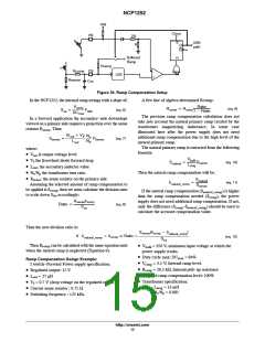
Figure 34. Ramp Compensation Setup
In the NCP1252, the internal ramp swings with a slope of:
A few line of algebra determined Rcomp:
Vramp
Ratio
Rcomp + R
(eq. 9)
ramp 1 * Ratio
Sint
+
FSW
(eq. 6)
DCmax
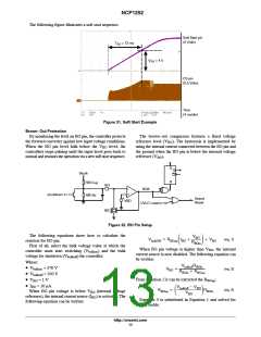
The previous ramp compensation calculation does not
take into account the natural primary ramp created by the
transformer magnetizing inductance. In some case
illustrated here after the power supply does not need
additional ramp compensation due to the high level of the
natural primary ramp.
In a forward application the secondary−side downslope
viewed on a primary side requires a projection over the sense
resistor R
. Thus:
sense
(Vout ) Vf)
Ns
Np
Ssense
+
Rsense
(eq. 7)
Lout
The natural primary ramp is extracted from the following
formula:
where:
• V is output voltage level
out
Vbulk
Lmag
• V the freewheel diode forward drop
f
Snatural
+
Rsense
(eq. 10)
• L , the secondary inductor value
out
Then the natural ramp compensation will be:
• N /N the transformer turn ratio
s
p
• R
: the sense resistor on the primary side
Snatural
Ssense
sense
dnatural_comp
+
(eq. 11)
Assuming the selected amount of ramp compensation to
be applied is δ , then we must calculate the division ratio
comp
If the natural ramp compensation (δ
) is higher
), the power
natural_comp
to scale down S accordingly:
int
than the ramp compensation needed (δ
comp
R
sensedcomp
Sint
supply does not need additional ramp compensation. If not,
Ratio +
(eq. 8)
only the difference (δ
−δ
) should be used to
calculate the accurate compensation value.
comp natural_comp
Thus the new division ratio is:
S
sense(dcomp * dnatural_comp
)
if dnatural_comp t dcomp å Ratio +
(eq. 12)
Sint
Then R
can be calculated with the same equation used
• V
= 350 V, minimum input voltage at which the
power supply works.
comp
bulk
when the natural ramp is neglected (Equation 9).
• Duty cycle max: DC
= 84%
max
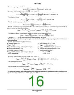
Ramp Compensation Design Example:
2 switch−Forward Power supply specification:
• V
• R
= 3.5 V, Internal ramp level.
ramp
= 26.5 kW, Internal pull−up resistance
• Regulated output: 12 V
ramp
• Targeted ramp compensation level: 100%
• Transformer specification:
• L = 27 mH
out
• V = 0.7 V (drop voltage on the regulated output)
f
− L
= 13 mH
mag
• Current sense resistor : 0.75 W
• Switching frequency : 125 kHz
− N /N = 0.085
s
p
http://onsemi.com
15

 ONSEMI [ ONSEMI ]