NCP1252
Application Information
Introduction
V ) after a minimum internal time delay of 120 ms
CC(on)
The NCP1252 hosts a high−performance current−mode
controller specifically developed to drive power supplies
designed for the ATX and the adapter market:
• Current Mode operation: implementing peak
current−mode control topology, the circuit offers
UC384X−like features to build rugged power supplies.
• Adjustable switching frequency: a resistor to ground
precisely sets the switching frequency between 50 kHz
and a maximum of 500 kHz. There is no
(SS
). But also when the brown−out pin is reset
delay
without in that case timer delay. This internal time
delay gives extra time to the PFC to be sure that the
output PFC voltage is in regulation. The soft start pin is
grounded until the internal delay is ended.
• Shutdown: if an external transistor brings the BO pin
down, the controller is shut down, but all internal
biasing circuits are alive. When the pin is released, a
new soft−start sequence takes place.
synchronization capability.
• Brown−Out protection: BO pin permanently monitors
• Internal frequency jittering: Frequency jittering
softens the EMI signature by spreading out peak energy
within a band 5% from the center frequency.
a fraction of the input voltage. When this image is
below the V threshold, the circuit stays off and does
BO
not switch. As soon the voltage image comes back
within safe limits, the pulses are re−started via a
start−up sequence including soft−start. The hysteresis is
implemented via a current source connected to the BO
• Wide Vcc excursion: the controller allows operation
up to 28 V continuously and accepts transient voltage
up to 30 V during 10 ms with I
< 20 mA
VCC
pin; this current source sinks a current (I ) from the
BO
• Gate drive clamping: a lot of powers MOSFETs do
not allow their driving voltage to exceed 20 V. The
controller includes a low−loss clamping voltage which
prevents the gate from going beyond 15 V typical.
pin to the ground. As the current source status depends
on the brown−out comparator, it can easily be used for
hysteresis purposes. A transistor pulling down the BO
pin to ground will shut−off the controller. Upon release,
a new soft−start sequence takes place.
• Low startup−current: reaching a low no−load standby
power represents a difficult exercise when the
• Internal ramp compensation: a simple resistor
connected from the CS pin to the sense resistor allows
the designer to inject ramp compensation inside his
design.
• Skip cycle feature: When the power supply loads are
decreasing to a low level, the duty cycle also decreases
to the minimum value the controller can offer. If the
output loads disappear, the converter runs at the
controller requires an external, lossy, resistor connected
to the bulk capacitor. The start−up current is guaranteed
to be less than 100 mA maximum, helping the designer
to reach a low standby power level.
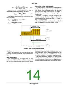
• Short−circuit protection: by monitoring the CS pin
voltage when it exceeds 1 V (maximum peak current),
the controller detects a fault and starts an internal
digital timer. On the condition that the digital timer
elapses, the controller will permanently latch−off. This
allows accurate overload or short−circuit detection
which is not dependant on the auxiliary winding. Reset
minimum duty cycle fixed by the propagation delay and
driving blocks. It often delivers too much energy to the
secondary side and it trips the voltage supervisor. To
avoid this problem, the FB is allowed to impose the min
occurs when: a) a BO reset is sensed, b) V is cycled
CC
t
down to ~ V and it further decreases down to
ON
f
down to V
level. If the short circuit or the fault
CC(min)
V
skip
, zero duty cycle is imposed. This mode helps to
disappear before the fault timer ends, the fault timer is
reset only if the CS pin voltage level is below 1 V at
least during 3 switching frequency periods. This delay
before resetting the fault timer prevents any false or
missing fault or over load detection.
ensure no−load outputs conditions as requested by
recently updated ATX specifications. Please note that
the converter first goes to min t before going to zero
ON
duty cycle: normal operation is thus not disturbed. The
following figure illustrates the different mode of
operation versus the FB pin level.
• Adjustable soft−start: the soft−start is activated upon
a start−up sequence (V going−up and crossing
CC
http://onsemi.com
10

 ONSEMI [ ONSEMI ]