NCP1251
vcc
vdrv
ilprim
3
1
2
1
V (t)
23.6
14.8
6.05
15.9
9.90
3.89
4.32
3.35
2.38
1.41
cc
VDRV
(t)
(t)
2
−2.72 −2.12
SS
IL
p
−11.5 −8.13 445m
3
500u
1.50m
2.50m
3.50m
4.50m
time in seconds
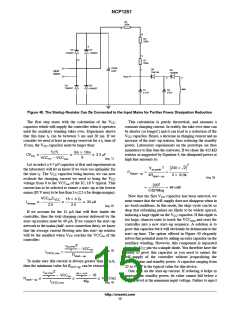
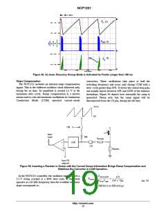
Figure 45. An Auto−Recovery Hiccup Mode is Activated for Faults Longer than 100 ms
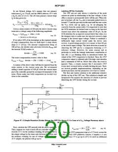
Slope Compensation
converters. These oscillations take place at half the
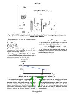
The NCP1251 includes an internal ramp compensation
signal. This is the buffered oscillator clock delivered only
during the on time. Its amplitude is around 2.5 V at the
maximum duty−cycle. Ramp compensation is a known
means used to cure sub harmonic oscillations in Continuous
Conduction Mode (CCM) operated current−mode
switching frequency and occur only during CCM with a
duty−cycle greater than 50%. To lower the current loop gain,
one usually injects between 50% and 100% of the inductor
downslope. Figure 46 depicts how internally the ramp is
generated. Please note that the ramp signal will be
disconnected from the CS pin, during the off time.
2.5 V
0V
ON
latch
reset
20k
Rcomp
+
LEB
CS
−
Rsense
from FB
setpoint
Figure 46. Inserting a Resistor in Series with the Current Sense Information Brings Ramp Compensation and
Stabilizes the Converter in CCM Operation.
In the NCP1251 controller, the oscillator ramp features a
2.5 V swing reached at a 80% duty−ratio. If the clock
operates at a 65 kHz frequency, then the available oscillator
slope corresponds to:
Vramp,peak
2.5
Sramp
+
+
(eq. 10)
0.8 15m
DmaxTSW
+ 208 kVńs or 208 mVńms
http://onsemi.com
19

 ONSEMI [ ONSEMI ]