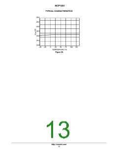
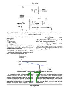
SUM2
NCP1251
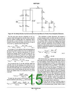
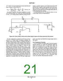
RoppU
swings to:
Vout during toff
−N V in during ton
VCC
aux
This p oin t will
be adjusted to
reduce the ref
at hi line to the
desired level.
from FB
reset
VDD
K1
−
OPP
ref
CS
+
K2
Iopp
0.8 V
$5%
R oppL
ref = 0.8 V + VOPP
(V O P P is negativ e)
Figure 42. The OPP Circuitry Affects the Maximum Peak Current Set Point by Summing a Negative Voltage to the
Internal Voltage Reference
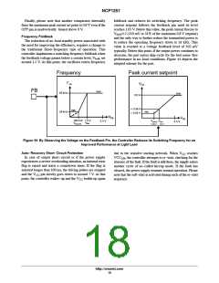
Let us assume that we have the following converter
characteristics:
0.16
67.5
(eq. 8)
Div +
[ 2.4m
If we arbitrarily fix the pull−down resistor R
to 1 kW,
V
out
= 19 V
OPPL
then the upper resistor can be obtained by:
V = 85 to 265 V
in
rms
N = N :N = 1:0.25
1
p
s
67.5 * 0.16
(eq. 9)
ROPPU
+
[ 421 kW
N = N :N = 1:0.18
2
p
aux
0.16ń1k
Given the turns ratio between the primary and the auxiliary
windings, the on−time voltage at high line (265 Vac) on the
auxiliary winding swings down to:
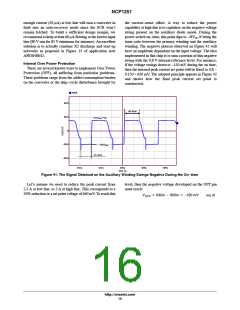
If we now plot the peak current set point obtained by
implementing the recommended resistor values, we obtain
the following curve (Figure 43):
Vaux + −N2Vin,max + −0.18 375 + −67.5 V
(eq. 7)
To obtain a level as imposed by Equation 6, we need to
install a divider featuring the following ratio:
Peak current
setpoint
100%
80%
Vbulk
375
Figure 43. The Peak Current Regularly Reduces Down to 20% at 375 Vdc
The OPP pin is surrounded by Zener diodes stacked to
protect the pin against ESD pulses. These diodes accept
some peak current in the avalanche mode and are designed
to sustain a certain amount of energy. On the other side,
negative injection into these diodes (or forward bias) can
cause substrate injection which can lead to an erratic circuit
behavior. To avoid this problem, the pin is internally
clamped slightly below –300 mV which means that if more
current is injected before reaching the ESD forward drop,
then the maximum peak reduction is kept to 40%. If the
voltage finally forward biases the internal zener diode, then
care must be taken to avoid injecting a current beyond
–2 mA. Given the value of R
present example.
, there is no risk in the
OPPU
http://onsemi.com
17

 ONSEMI [ ONSEMI ]