NCP1239
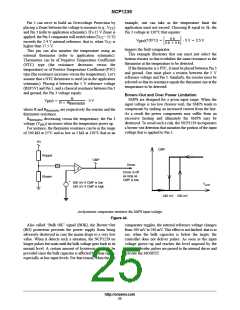
Pin 3 can serve to build an Overvoltage Protection by
placing a Zener between the voltage to measure (e.g., V
example, one can take as the temperature limit the
application must not exceed. Choosing R equal to 5k, the
)
CC
and Pin 3 (refer to application schematic). If a 15 V Zener is
applied, the Pin 3 comparator will switch when (V − 15 V)
Pin 3 voltage at 130°C that equates:
CC
5 k
5 k ) 5 k
(130°C) + ƪ
V
pin3
ƫ@ 5 V + 2.5 V
exceeds the 2.4 V internal reference, that is, when V is
CC
higher than 17.5 V.
triggers the fault comparator.
This pin can also monitor the temperature using an
external thermistor (refer to application schematic).
Thermistors can be of Negative Temperature Coefficient
(NTC) type (the resistance decreases versus the
temperature) or of Positive Temperature Coefficient (PTC)
type (the resistance increases versus the temperature). Let’s
assume that a NTC thermistor is used (as in the application
schematic). Placing it between the 5 V reference voltage
(REF5V) and Pin 3, and a classical resistance between Pin 3
and ground, the Pin 3 voltage equals:
This example illustrates that one must just select the
bottom resistor so that it exhibits the same resistance as the
thermistor at the temperature to be detected.
If the thermistor is a PTC, it must be placed between Pin 3
and ground. One must place a resistor between the 5 V
reference voltage and Pin 3. Similarly, the resistor must be
selected so that its resistance equals the thermistor one at the
temperature to be detected.
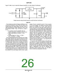
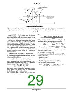
Brown−Out and Over Power Limitation
R
SMPS are designed for a given input range. When the
input voltage is too low (brown−out), the SMPS tends to
compensate by sinking an increased current from the line.
As a result the power components may suffer from an
excessive heating and ultimately the SMPS may be
destroyed. To avoid such a risk, the NCP1239 incorporates
a brown−out detection that monitors the portion of the input
voltage that is applied to Pin 5.
V
pin3
+
@ 5 V
R ) R
thermistor
where R and R
are respectively the resistor and the
thermistor
thermistor resistance.
decreasing versus the temperature, the Pin 3
R
thermistor
voltage (V ) increases when the temperature grows up.
pin3
For instance, the thermistor resistance can be in the range
of 500 kꢂ at 25°C and as low as 5 kꢂ at 130°C that as an
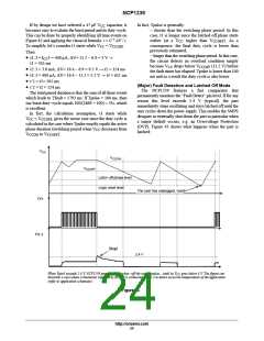
HV
CMP
Rupper
CMP
Driver
5
+
−
Driver is off
as long as
CMP is low
Rlower
+
500 mV if CMP is low
240 mV if CMP is high
V
pin5
240 mV 500 mV
An hysteresis comparator monitors the SMPS input voltage
Figure 44.
Also called “Bulk OK” signal (BOK), the Brown−Out
(BO) protection prevents the power supply from being
adversely destroyed in case the mains drops to a very low
value. When it detects such a situation, the NCP1239 no
longer pulses but waits until the bulk voltage goes back to its
normal level. A certain amount of hysteresis needs to be
provided since the bulk capacitor is affected by some ripple,
especially at low input levels. For that reason, when the BO
comparator toggles, the internal reference voltage changes
from 500 mV to 240 mV. This effect is not latched: that is to
say, when the bulk capacitor is below the target, the
controller does not deliver pulses. As soon as the input
voltage grows−up and reaches the level imposed by the
resistive divider, pulses are passed to the internal driver and
activate the MOSFET.
http://onsemi.com
25

 ONSEMI [ ONSEMI ]