NCP1239
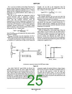
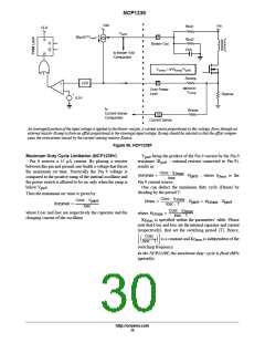
Actual Peak Current
Low Input
Voltage
ꢃI
HL
Vopl/Rsense
ꢃI
LL
Wished Maximum
Peak Current
High Input
Voltage
ꢃ t
ꢃ t
The propagation delay (Dt) produces overcurrents (DILL at low line, DIHL at high line in the figure) that are proportional to the input
voltage. As a consequence, the actual maximum current and then the power limit gets higher when the AC line increases.
Figure 49.
Then,
Vocp
Rsense
Vin @ ꢄ t
Lp
Imax +
)
, where Vin is the converter
Vopl * (Rcomp @ 80 ꢁ AńV @ k
@ Vin)
BO
Ipth +
input voltage and ꢃt is the total delay in turning off the
power switch.
The NCP1239 enables the compensation of the second
term in the Imax equation for a precise limitation of the peak
Rsense
Taking into account the overcurrent resulting from the
propagation delays, the maximum current is finally:
Rcomp @ 80 ꢁ AńV @ k
@ Vin
current. A current source (I ) proportional to the Pin 5
voltage flows out of Pin 9. Since Pin 5 receives a voltage
proportional to the input voltage for brown−out detection,
Vocp
Rsense
BO
pin9
Vin @ ꢄt
I max +
*
)
Rsense
Lp
Rcomp @ 80 ꢁAńV @ k
BO
ꢄ
t
Choosing Rcomp so that
)
,
I
is proportional to the input voltage too. An external
pin9
Rsense
Lp
resistor Rcomp can be connected between Pin 9 and the
positive terminal of Rsense, so that Pin 9 monitors the
following voltage:
the current limit is made constant in the whole input voltage
range (Imax = Vocp/Rsense).
As an example, let’s assume that:
V
pin9
+ [Rsense @ (Ip ) I
)] ) (Rcomp @ I )
pin9 pin9
− the minimum input voltage for operation is 100 V =>
k
=0.5/100=0.005,
BO
I
being small compared to the inductor current, the Pin 9
pin9
voltage simplifies as follows:
− Rsense is 0.25 ꢂ,
V
pin9
+ (Rsense @ Ip) ) (Rcomp @ I )
pin9
− Lp=500 ꢁ H,
− The total propagation delays are ꢃt = 350 ns,
Then, the Rcomp resistor should be:
I
is proportional to the Pin 5 voltage (80 ꢁ A/V*V
–
pin9
pin5
see parameters specification table) and V
is a portion of
pin5
the input voltage (V
= k *Vin). Finally,
BO
ꢄt @ Rsense
80 ꢁ @ k @ Lp
350 n @ 0.25
80 ꢁ @ 0.005 @ 500 m
.
[ 438 ꢂ
pin5
Rcomp +
+
BO
I
+ 80 ꢁAńV @ k
@ Vin
BO
pin9
The voltage V
is compared to the internal reference
pin9
Vocp. When V
reaches Vocp, the corresponding
pin9
threshold current (Ipth) is deducted from:
Vopl + (Rsense @ Ipth) ) (Rcomp @ 80 ꢁ AńV @ k
@ Vin)
BO
http://onsemi.com
29

 ONSEMI [ ONSEMI ]