NCP1207
hosts a dedicated overload detection circuitry. Once
• If the power consumption budget is really too high for the
activated, this circuitry imposes to deliver pulses in a burst
manner with a low duty−cycle. The system recovers when
the fault condition disappears.
DSS alone, connect a diode between the auxiliary
winding and the V pin which will disable the DSS
CC
operation (V u 10 V).
CC
During the startup phase, the peak current is pushed to the
maximum until the output voltage reaches its target and the
feedback loop takes over. This period of time depends on
normal output load conditions and the maximum peak
current allowed by the system. The time−out used by this IC
The SOIC package offers a 178°C/W thermal resistor.
Again, adding some copper area around the PCB footprint
will help decrease this number: 12 mm 12 mm to drop
R
qJA
down to 100°C/W with 35 mm copper thickness (1 oz.)
or 6.5 mm 6.5 mm with 70 mm copper thickness (2 oz.).
As one can see, we do not recommend using the SO−8
package and the DSS if the part operates at high switching
frequencies. In that case, an auxiliary winding is the best
solution.
works with the V decoupling capacitor: as soon as the
CC
V
CC
decreases from the VCC
level (typically 12 V) the
OFF
device internally watches for an overload current situation.
If this condition is still present when the VCC level is
ON
reached, the controller stops the driving pulses, prevents the
self−supply current source to restart and puts all the circuitry
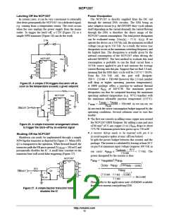
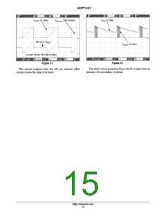
Overload Operation
In applications where the output current is purposely not
controlled (e.g. wall adapters delivering raw DC level), it is
interesting to implement a true short−circuit protection. A
short−circuit actually forces the output voltage to be at a low
level, preventing a bias current to circulate in the
Optocoupler LED. As a result, the FB pin level is pulled up
to 4.2 V, as internally imposed by the IC. The peak current
setpoint goes to the maximum and the supply delivers a
rather high power with all the associated effects. Please note
that this can also happen in case of feedback loss, e.g. a
broken Optocoupler. To account for this situation, NCP1207
in standby, consuming as little as 330 mA typical (I
CC3
parameter). As a result, the V level slowly discharges
CC
toward 0. When this level crosses 5.3 V typical, the
controller enters a new startup phase by turning the current
source on: V rises toward 12 V and again delivers output
CC
pulses at the VCC
crossing point. If the fault condition
OFF
has been removed before VCC approaches, then the IC
ON
continues its normal operation. Otherwise, a new fault cycle
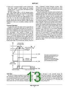
takes place. Figure 28 shows the evolution of the signals in
presence of a fault.
V
CC
REGULATION
OCCURS HERE
12 V
LATCH−OFF
PHASE
10 V
5.3 V
TIME
If the fault is relaxed during the V
CC
DRV
natural fall down sequence, the IC
automatically resumes.
If the fault still persists when V
DRIVER
PULSES
CC
reached VCC , then the controller
ON
cuts everything off until recovery.
TIME
TIME
INTERNAL
FAULT FLAG
FAULT IS
RELAXED
STARTUP PHASE
FAULT OCCURS HERE
Figure 28.
Soft−Start
1.0 V). The soft−start is also activated during the
overcurrent burst (OCP) sequence. Every restart attempt is
followed by a soft−start activation. Generally speaking, the
The NCP1207 features an internal 1 ms soft−start to soften
the constraints occurring in the power supply during startup.
It is activated during the power on sequence. As soon as V
soft−start will be activated when V ramps up either from
CC
CC
reaches VCC
, the peak current is gradually increased
zero (fresh power−on sequence) or 5.3 V, the latch−off
voltage occurring during OCP.
OFF
from nearly zero up to the maximum clamping level (e.g.
http://onsemi.com
13

 ONSEMI [ ONSEMI ]