NCP1207
The DSS behavior actually depends on the internal IC
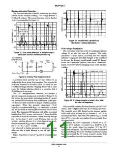
When using Figure17 option, it is important to check
the absence of any negative ringing that could occur
on pin 8. The resistor in series should help to damp
any parasitic LC network that would ring when
suddenly applying the power to the IC. Also, since
the power disappears during 10 ms (half−wave
consumption and the MOSFET’s gate charge Qg. If we
select a MOSFET like the MTP2N60E, Qg equals 22 nC
(max). With a maximum switching frequency selected at
75 kHz, the average power necessary to drive the MOSFET
(excluding the driver efficiency and neglecting various
voltage drops) is:
rectification), CV should be calculated to supply
CC
the IC during these holes in the supply
Fsw Qg V with:
CC
3. Permanently force the V level above V
with
CCH
CC
Fsw = maximum switching frequency
Qg = MOSFET’s gate charge
an auxiliary winding. It will automatically
disconnect the internal startup source and the IC will
be fully self−supplied from this winding. Again, the
total power drawn from the mains will significantly
decrease. Make sure the auxiliary voltage never
exceeds the 16 V limit.
V
CC
= V level applied to the gate
GS
To obtain the output current, simply divide this result by
: I = F Qg = 1.6 mA. The total standby power
V
CC driver
SW
consumption at no−load will therefore heavily rely on the
internal IC consumption plus the above driving current
(altered by the driver’s efficiency). Suppose that the IC is
supplied from a 350 VDC line. The current flowing through
pin 8 is a direct image of the NCP1207 consumption
(neglecting the switching losses of the HV current source).
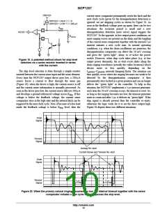
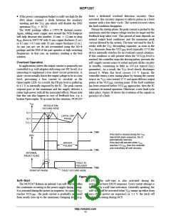
Skipping Cycle Mode
The NCP1207 automatically skips switching cycles when
the output power demand drops below a given level. This is
accomplished by monitoring the FB pin. In normal
operation, pin 2 imposes a peak current accordingly to the
load value. If the load demand decreases, the internal loop
asks for less peak current. When this setpoint reaches a
determined level, the IC prevents the current from
decreasing further down and starts to blank the output
pulses: the IC enters the so−called skip cycle mode, also
named controlled burst operation. The power transfer now
depends upon the width of the pulse bunches (Figure 18) and
follows the following formula:
If I
equals 2.3 mA @ T = 60°C, then the power
CC2
J
dissipated (lost) by the IC is simply: 350 V x 2.3 mA =
805 mW. For design and reliability reasons, it would be
interested to reduce this source of wasted power that
increase the die temperature. This can be achieved by using
different methods:
1. Use a MOSFET with lower gate charge Qg.
2. Connect pin 8 through a diode (1N4007 typically) to
one of the mains input. The average value on pin 8
1
2
@ Lp @ Ip2 @ Fsw @ D
with:
V
mainsPEAK @ 2
burst
becomes
. Our power contribution
p
example drops to: 223 V x 2.3 mA = 512 mW. If a
resistor is installed between the mains and the diode,
you further force the dissipation to migrate from the
package to the resistor. The resistor value should
account for low−line startups.
Lp = primary inductance
Fsw = switching frequency within the burst
Ip = peak current at which skip cycle occurs
D
burst
= burst width / burst recurrence
HV
1N4007
MAX PEAK
CURRENT
NORMAL CURRENT
MODE OPERATION
300
200
100
0
5
1
2
C
bulk
1
2
3
4
8
MAINS
6
SKIP CYCLE
CURRENT LIMIT
7
6
5
Figure 17. A simple diode naturally reduces the
average voltage on pin 8
WIDTH
RECURRENCE
Figure 18. The skip cycle takes place at low peak
currents which guaranties noise free operation
http://onsemi.com
9

 ONSEMI [ ONSEMI ]