NCP1207
Latching Off the NCP1207
Power Dissipation
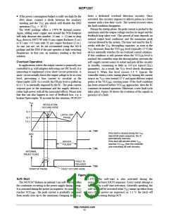
In certain cases, it can be very convenient to externally
shut down permanently the NCP1207 via a dedicated signal,
e.g. coming from a temperature sensor. The reset occurs
when the user unplugs the power supply from the mains
outlet. To trigger the latch−off, a CTN (Figure 25) or a
simple NPN transistor (Figure 26) can do the work.
The NCP1207 is directly supplied from the DC rail
through the internal DSS circuitry. The DSS being an
auto−adaptive circuit (e.g. the ON/OFF duty−cycle adjusts
itself depending on the current demand), the current flowing
through the DSS is therefore the direct image of the
NCP1207 current consumption. The total power dissipation
can be evaluated using: (V
* 11 V) @ I . If we
HVDC
CC2
CTN
operate the device on a 250 Vac rail, the maximum rectified
voltage can go up to 350 Vdc. As a result, the worse case
dissipation occurs at the maximum switching frequency and
the highest line. The dissipation is actually given by the
internal consumption of the NCP1207 when driving the
selected MOSFET. The best method to evaluate this total
consumption is probably to run the final circuit from a
50 Vdc source applied to pin 8 and measure the average
current flowing into this pin. Suppose that we find 2.0 mA,
meaning that the DSS duty−cycle will be 2.0/7.0 = 28.6%.
From the 350 Vdc rail, the part will dissipate:
350 V @ 2.0 mA + 700 mW (however this 2.0 mA number
will drop at higher operating junction temperatures).
A DIP8 package offers a junction−to−ambient thermal
NCP1207
Aux
1
2
3
4
8
7
6
5
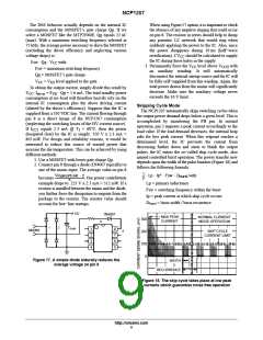
Figure 25. A simple CTN triggers the latch−off as
soon as the temperature exceeds a given setpoint
resistance R
of 100°C/W. The maximum power
qJA
dissipation can thus be computed knowing the maximum
operating ambient temperature (e.g. 70°C) together with
the maximum allowable junction temperature (125°C):
NCP1207
Aux
1
2
3
4
8
7
6
5
T
* T
Amax
Jmax
P
+
t 550 mW. As we can see, we
max
R
qJA
ON/OFF
do not reach the worse consumption budget imposed by the
operating conditions. Several solutions exist to cure this
trouble:
• The first one consists in adding some copper area around
the NCP1207 DIP8 footprint. By adding a min pad area
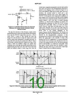
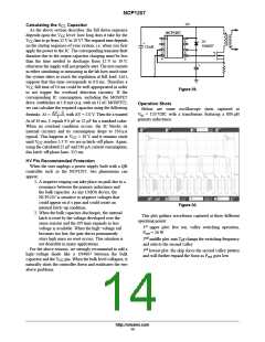
Figure 26. A simple transistor arrangement allows
to trigger the latch−off by an external signal
2
of 80 mm of 35 mm copper (1 oz.) R
drops to about
qJA
75°C/W. Maximum power then grows up to 730 mW.
• A resistor Rdrop needs to be inserted with pin 8 to
a) avoid negative spikes at turn−off (see below)
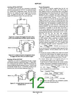
Shutting Off the NCP1207
Shutdown can easily be implemented through a simple
NPN bipolar transistor as depicted by Figure 27. When OFF,
Q1 is transparent to the operation. When forward biased, the
transistor pulls the FB pin to ground (V
permanently disables the IC. A small time constant on the
transistor base will avoid false triggering (Figure 27).
b) split the power budget between this resistor and the
package. The resistor is calculated by leaving at least 50 V
on pin 8 at minimum input voltage (suppose 100 Vdc in
≈ 200 mV) and
CE(sat)
V
* 50 V
7.0 mA
bulkmin
our case): R
v
t 7.1 kW. The
drop
power dissipated by the resistor is thus:
NCP1207
P
+ V
2ńR
drop
dropRMS
drop
2
1
2
3
4
8
7
6
5
Ǹ
DSS
ǒI
duty * cycleǓ
@ R
@
DSS
drop
+
10 k
1
R
drop
Ǹ
Q1
ON/OFF
ǒ7.0 mA @ 7.1 kW @ 0.286Ǔ2
3
2
+
+ 99.5 mW
10 nF
7.1 kW
Please refer to the application note AND8069 available
from www.onsemi.com/pub/ncp1200.
Figure 27. A simple bipolar transistor totally
disables the IC
http://onsemi.com
12

 ONSEMI [ ONSEMI ]