NCP1207
HV
Calculating the V Capacitor
CC
As the above section describes, the fall down sequence
depends upon the V level: how long does it take for the
NCP1207
CC
V
line to go from 12 V to 10 V? The required time depends
1
2
3
4
8
CC
D1
1N4007
+
on the startup sequence of your system, i.e. when you first
apply the power to the IC. The corresponding transient fault
duration due to the output capacitor charging must be less
than the time needed to discharge from 12 V to 10 V,
otherwise the supply will not properly start. The test consists
in either simulating or measuring in the lab how much time
the system takes to reach the regulation at full load. Let’s
suppose that this time corresponds to 6.0 ms. Therefore a
Cbulk
7
6
5
+
V
fall time of 10 ms could be well appropriated in order
CC
Figure 29.
to not trigger the overload detection circuitry. If the
corresponding IC consumption, including the MOSFET
drive, establishes at 1.8 mA (e.g. with an 11 nC MOSFET),
we can calculate the required capacitor using the following
DV @ C
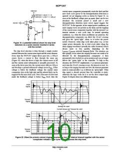
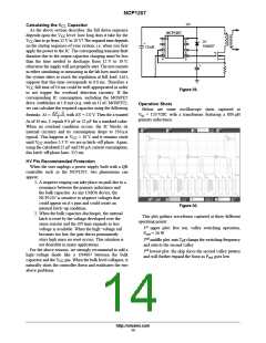
Operation Shots
Below are some oscilloscope shots captured at
= 120 VDC with a transformer featuring a 800 mH
V
formula: Dt +
, with DV = 2.0 V. Then for a wanted
in
i
primary inductance.
Dt of 10 ms, C equals 9.0 mF or 22 mF for a standard value.
When an overload condition occurs, the IC blocks its
internal circuitry and its consumption drops to 330 mA
typical. This happens at V = 10 V and it remains stuck
CC
until V reaches 5.3 V: we are in latch−off phase. Again,
CC
using the calculated 22 mF and 330 mA current consumption,
this latch−off phase lasts: 313 ms.
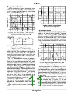
HV Pin Recommended Protection
When the user unplugs a power supply built with a QR
controller such as the NCP1207, two phenomena can
appear:
1. A negative ringing can take place on pin8 due to a
resonance between the primary inductance and
the bulk capacitor. As any CMOS device, the
NCP1207 is sensitive to negative voltages that
could appear on it’s pins and could create an
internal latch−up condition.
Figure 30.
2. When the bulk capacitor discharges, the internal
latch is reset by the voltage developed over the
sense resistor and the ON time expands as less
voltage is available. When the high−voltage rail
becomes too low, the gate drives permanently
stays high since no reset occurs. This situation is
not desirable in many applications.
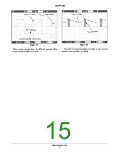
This plot gathers waveforms captured at three different
operating points:
st
1
upper plot: free run, valley switching operation,
= 26 W
P
out
nd
2
middle plot: min T clamps the switching frequency
off
and selects the second valley
For the above reasons, we strongly recommend to add a
high−voltage diode like a 1N4007 between the bulk
rd
3
lowest plot: the skip slices the second valley pattern
and will further expand the burst as P goes low
out
capacitor and the V pin. When the bulk level collapses, it
CC
naturally shuts the controller down and eradicates the two
above problems.
http://onsemi.com
14

 ONSEMI [ ONSEMI ]