NCP1207
Demagnetization Detection
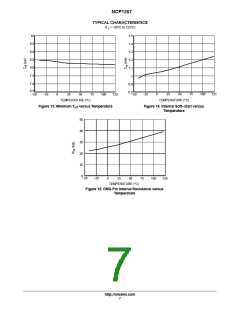
400
300
200
100
0
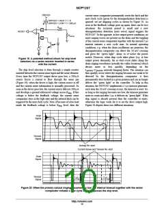
The core reset detection is done by monitoring the voltage
activity on the auxiliary winding. This voltage features a
FLYBACK polarity. The typical detection level is fixed at
50 mV as exemplified by Figure 21.
7.0
POSSIBLE
5.0
RE−STARTS
3.0
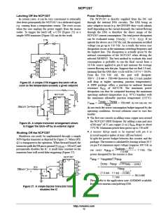
Figure 23. The NCP1207 Operates in
Borderline / Critical Operation
1.0
50 mV
0 V
−1.0
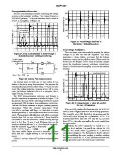
Overvoltage Protection
The overvoltage protection works by sampling the plateau
voltage 4.5 ms after the turn−off sequence. This delay
guarantees a clean plateau, providing that the leakage
inductance ringing has been fully damped. If this would not
be the case, the designer should install a small RC damper
across the transformer primary inductance connections.
Figure 24 shows where the sampling occurs on the auxiliary
winding.
Figure 21. Core reset detection is done through a
dedicated auxiliary winding monitoring
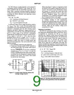
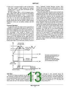
TO INTERNAL
COMPARATOR
R
R
dem
esd
1
2
1
5
4
R
ESD2
ESD1
4
int
Aux
3
SAMPLING HERE
8.0
R
+ R = 28 k
int
esd
Figure 22. Internal Pad Implementation
6.0
4.0
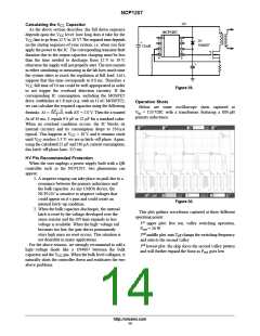
An internal timer prevents any re−start within 8.0 ms
further to the driver going−low transition. This prevents the
switching frequency to exceed (1 / (T + 8.0 ms)) but also
ON
avoid false leakage inductance tripping at turn−off. In some
cases, the leakage inductance kick is so energetic, that a
slight filtering is necessary.
2.0
4.5 ms
The 1207 demagnetization detection pad features a
specific component arrangement as detailed by Figure 22. In
this picture, the zener diodes network protect the IC against
any potential ESD discharge that could appear on the pins.
The first ESD diode connected to the pad, exhibits a parasitic
capacitance. When this parasitic capacitance (10 pF
0
Figure 24. A voltage sample is taken 4.5 ms after
the turn−off sequence
When an OVP condition has been detected, the NCP1207
enters a latch−off phase and stops all switching operations.
The controller stays fully latched in this position and the
DSS is still active, keeping the V between 5.3 V/12 V as
in normal operations. This state lasts until the V is cycled
down 4 V, e.g. when the user unplugs the power supply from
the mains outlet.
By default, the OVP comparator is biased to a 5 V
reference level and pin 1 is routed via a divide by 1.44
typically) is combined with R , a re−start delay is created
dem
and the possibility to switch right in the drain−source wave
exists. This guarantees QR operation with all the associated
CC
benefits (low EMI, no turn−on losses etc.). R
should be
dem
CC
calculated to limit the maximum current flowing through
pin 1 to less than +3 mA/−2 mA. If during turn−on, the
auxiliary winding delivers 30 V (at the highest line level),
then the minimum R
value is defined by:
dem
(30 V + 0.7 V) / 2 mA = 14.6 kW.
network. As a result, when V
reaches 7.2 V, the OVP
pin1
This value will be further increased to introduce a re−start
delay and also a slight filtering in case of high leakage
energy.
comparator is triggered. The threshold can thus be adjusted
by either modifying the power winding to auxiliary winding
turn ratios to match this 7.2 V level, or insert a resistor from
pin1 to ground to cope with your design requirement.
Figure 23 portrays a typical V shot at nominal output
DS
power.
http://onsemi.com
11

 ONSEMI [ ONSEMI ]