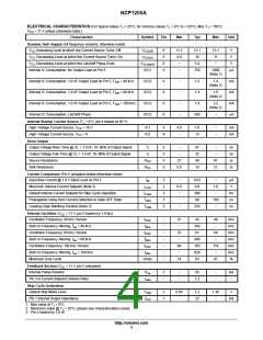
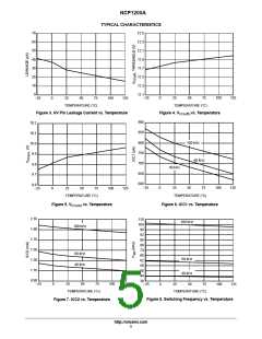
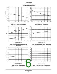
NCP1200A
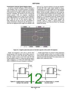
HV
mains
1
2
3
4
8
7
6
5
Cbulk
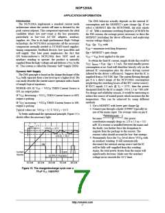
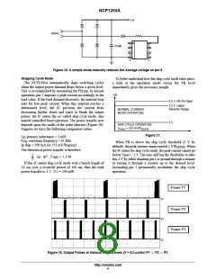
Figure 16. A simple diode naturally reduces the average voltage on pin 8
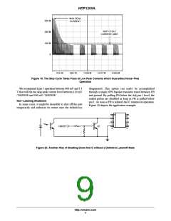
Skipping Cycle Mode
To better understand how this skip cycle mode takes place,
a look at the operation mode versus the FB level
immediately gives the necessary insight:
The NCP1200A automatically skips switching cycles
when the output power demand drops below a given level.
This is accomplished by monitoring the FB pin. In normal
operation, pin 2 imposes a peak current accordingly to the
load value. If the load demand decreases, the internal loop
asks for less peak current. When this setpoint reaches a
determined level, the IC prevents the current from
decreasing further down and starts to blank the output
pulses: the IC enters the so−called skip cycle mode, also
named controlled burst operation. The power transfer now
depends upon the width of the pulse bunches (Figure 18).
Suppose we have the following component values:
FB
4.2 V, FB Pin Open
3.2 V, Upper
Dynamic Range
NORMAL CURRENT
MODE OPERATION
1 V
SKIP CYCLE OPERATION
I
= 333 mV/R
SENSE
P(min)
Figure 17.
Lp, primary inductance = 1 mH
F
, switching frequency = 61 kHz
SW
When FB is above the skip cycle threshold (1 V by
default), the peak current cannot exceed 1 V/R . When
Ip skip = 200 mA (or 333 mV/R
)
SENSE
SENSE
The theoretical power transfer is therefore:
the IC enters the skip cycle mode, the peak current cannot go
below Vpin1 / 3.3. The user still has the flexibility to alter
this 1 V by either shunting pin 1 to ground through a resistor
or raising it through a resistor up to the desired level.
Grounding pin 1 permanently invalidates the skip cycle
operation.
1
2
@ Lp @ Ip2 @ F
+ 1.2 W
SW
If this IC enters skip cycle mode with a bunch length of
20 ms over a recurrent period of 100 ms, then the total
power transfer is: 1.2 . 0.2 = 240 mW.
Power P1
Power P2
Power P3
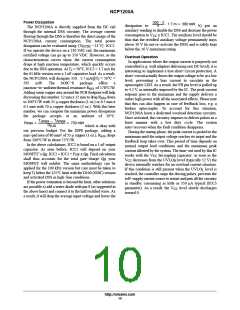
Figure 18. Output Pulses at Various Power Levels (X = 5.0 ms/div) P1 t P2 t P3
http://onsemi.com
8

 ONSEMI [ ONSEMI ]