NCP1200A
Power Dissipation
350 @ 2
@ 1.7 m + 380 mW
p
dissipation to:
b) put an
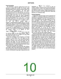
The NCP1200A is directly supplied from the DC rail
through the internal DSS circuitry. The average current
flowing through the DSS is therefore the direct image of the
NCP1200A current consumption. The total power
auxiliary winding to disable the DSS and decrease the power
consumption to V x ICC2. The auxiliary level should be
CC
thus that the rectified auxiliary voltage permanently stays
above 10 V (to not re−activate the DSS) and is safely kept
below the 16 V maximum rating.
dissipation can be evaluated using: (V
− 11 V) ICC2.
HVDC
If we operate the device on a 250 VAC rail, the maximum
rectified voltage can go up to 350 VDC. However, as the
characterization curves show, the current consumption
drops at high junction temperature, which quickly occurs
due to the DSS operation. At T = 50°C, ICC2 = 1.7 mA for
the 61 kHz version over a 1 nF capacitive load. As a result,
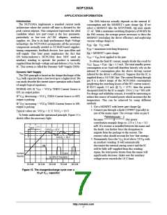
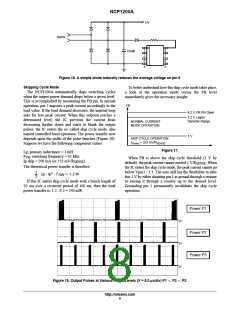
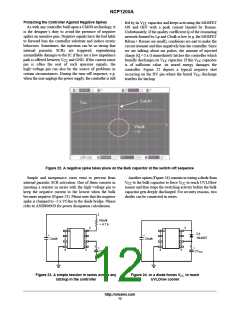
Overload Operation
In applications where the output current is purposely not
controlled (e.g. wall adapters delivering raw DC level), it is
interesting to implement a true short−circuit protection. A
short−circuit actually forces the output voltage to be at a low
level, preventing a bias current to circulate in the
optocoupler LED. As a result, the FB pin level is pulled up
to 4.2 V, as internally imposed by the IC. The peak current
setpoint goes to the maximum and the supply delivers a
rather high power with all the associated effects. Please note
that this can also happen in case of feedback loss, e.g. a
broken optocoupler. To account for this situation,
NCP1200A hosts a dedicated overload detection circuitry.
Once activated, this circuitry imposes to deliver pulses in a
burst manner with a low duty cycle. The system
auto−recovers when the fault condition disappears.
J
the NCP1200A will dissipate 350 . 1.7 mA@T = 50°C =
J
595
mW.
The
SOIC−8
package
offers
a
junction−to−ambientthermal resistance R
Adding some copper area around the PCB footprint will help
decreasing this number: 12 mm x 12 mm to drop R down
to 100°C/W with 35 m copper thickness (1 oz.) or 6.5 mm x
6.5 mm with 70 m copper thickness (2 oz.). With this later
number, we can compute the maximum power dissipation
the package accepts at an ambient of 50°C:
of 178°C/W.
qJA
qJA
T
T
Jmax * Amax
Pmax +
+ 750 mW
R
qJA
which is okay with
our previous budget. For the DIP8 package, adding a
min−pad area of 80 mm@ of 35 m copper (1 oz.), R
from 100°C/W to about 75°C/W.
In the above calculations, ICC2 is based on a 1 nF output
capacitor. As seen before, ICC2 will depend on your
MOSFET’s Qg: ICC2 ≈ ICC1 + F x Qg. Final calculation
shall thus accounts for the total gate−charge Qg your
MOSFET will exhibit. The same methodology can be
applied for the 100 kHz version but care must be taken to
During the startup phase, the peak current is pushed to the
maximum until the output voltage reaches its target and the
feedback loop takes over. This period of time depends on
normal output load conditions and the maximum peak
current allowed by the system. The time−out used by this IC
drops
qJA
SW
works with the V decoupling capacitor: as soon as the
CC
V
CC
decreases from the UVLO level (typically 12 V) the
device internally watches for an overload current situation.
If this condition is still present when the UVLO level is
reached, the controller stops the driving pulses, prevents the
self−supply current source to restart and puts all the circuitry
in standby, consuming as little as 350 mA typical (ICC3
H
L
keep T below the 125°C limit with the D100 (SOIC) version
J
and activated DSS in high−line conditions.
If the power estimation is beyond the limit, other solutions
are possible a) add a series diode with pin 8 (as suggested in
the above lines) and connect it to the half rectified wave. As
a result, it will drop the average input voltage and lower the
parameter). As a result, the V level slowly discharges
CC
toward 0.
http://onsemi.com
10

 ONSEMI [ ONSEMI ]