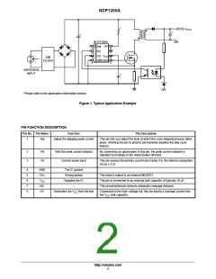
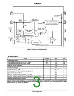
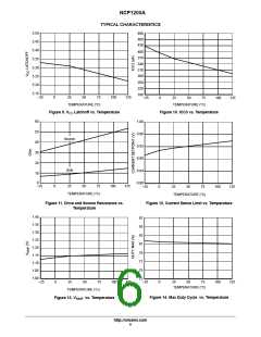
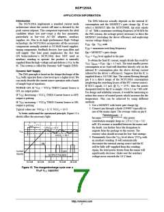
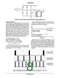
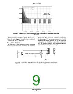
NCP1200A
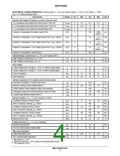
ELECTRICAL CHARACTERISTICS (For typical values T = 25°C, for min/max values T = 0°C to +125°C, Max T = 150°C,
J
J
J
V
CC
= 11 V unless otherwise noted.)
Characteristic
Dynamic Self−Supply (All frequency versions, otherwise noted)
Symbol
Pin
Min
Typ
Max
Unit
V
V
V
Increasing Level at which the Current Source Turns−Off
Decreasing Level at which the Current Source Turns−On
Decreasing Level at which the Latchoff Phase Ends
V
V
6
6
6
6
11.2
9.0
−
12.1
10
13.1
11
V
V
CC
CC
CC
CC(off)
CC(on)
V
5.4
750
−
V
CC(latch)
Internal IC Consumption, No Output Load on Pin 5
Internal IC Consumption, 1.0 nF Output Load on Pin 5, F
Internal IC Consumption, 1.0 nF Output Load on Pin 5, F
Internal IC Consumption, 1.0 nF Output Load on Pin 5, F
Internal IC Consumption, Latchoff Phase
ICC1
−
1000
(Note 1)
mA
= 40 kHz
= 60 kHz
= 100 kHz
ICC2
ICC2
ICC2
ICC3
6
6
6
6
−
−
−
−
1.2
1.4
1.9
350
1.4
(Note 2)
mA
mA
mA
mA
SW
SW
SW
1.6
(Note 2)
2.2
(Note 2)
−
Internal Startup Current Source (T > 0°C, pin 8 biased at 50 V)
J
High−Voltage Current Source, V = 10 V
IC1
IC2
8
8
4.0
−
7.0
13
−
−
mA
mA
CC
High−Voltage Current Source, V = 0
CC
Drive Output
Output Voltage Rise−Time @ CL = 1.0 nF, 10−90% of Output Signal
T
5
5
5
5
−
−
67
25
40
10
−
−
ns
ns
W
r
Output Voltage Fall−Time @ CL = 1.0 nF, 10−90% of Output Signal
T
f
Source Resistance
Sink Resistance
R
27
5.0
61
21
OH
R
W
OL
Current Comparator (Pin 5 unloaded unless otherwise noted)
Input Bias Current @ 1.0 V Input Level on Pin 3
I
3
3
3
3
3
−
0.8
−
0.02
0.9
−
1.0
−
mA
V
IB
Maximum Internal Current Setpoint (Note 3)
I
Limit
Default Internal Current Setpoint for Skip Cycle Operation
Propagation Delay from Current Detection to Gate OFF State
Leading Edge Blanking Duration (Note 3)
I
360
90
mV
ns
ns
Lskip
T
−
160
−
DEL
LEB
T
−
250
Internal Oscillator (V = 11 V, pin 5 loaded by 1.0 kW)
CC
Oscillation Frequency, 40 kHz Version
f
f
f
−
−
−
−
−
−
−
37
−
43
350
61
48
−
kHz
kHz
kHz
kHz
kHz
kHz
%
OSC
Built−in Frequency Jittering, f = 40 kHz
f
sw
jitter
Oscillation Frequency, 60 kHz Version
53
−
68
−
OSC
Built−in Frequency Jittering, f = 60 kHz
f
460
103
620
83
sw
jitter
Oscillation Frequency, 100 kHz Version
90
−
114
−
OSC
Built−in Frequency Jittering, f = 100 kHz
f
jitter
sw
Maximum Duty Cycle
Dmax
74
87
Feedback Section (V = 11 V, pin 5 unloaded)
CC
Internal Pullup Resistor
R
2
−
−
−
20
−
−
kW
up
Pin 3 to Current Setpoint Division Ratio
I
3.3
−
ratio
Skip Cycle Generation
Default Skip Mode Level
V
1
1
0.95
−
1.2
22
1.45
−
V
skip
Pin 1 Internal Output Impedance
Z
kW
out
1. Max value at T = 0°C.
J
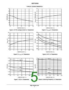
2. Maximum value @ T = 25°C, please see characterization curves.
J
3. Pin 5 loaded by 1.0 nF.
http://onsemi.com
4

 ONSEMI [ ONSEMI ]