NCP1200A
APPLICATION INFORMATION
Introduction
The DSS behavior actually depends on the internal IC
consumption and the MOSFET’s gate charge Qg. If we
select a MOSFET like the MTP2N60E, Qg max equals
22 nC. With a maximum switching frequency of 68 kHz for
the P60 version, the average power necessary to drive the
MOSFET (excluding the driver efficiency and neglecting
various voltage drops) is:
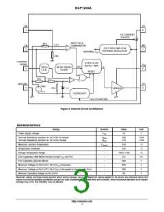
The NCP1200A implements a standard current mode
architecture where the switch−off time is dictated by the
peak current setpoint. This component represents the ideal
candidate where low part−count is the key parameter,
particularly in low−cost AC−DC adapters, auxiliary
supplies, etc. Due to its high−performance High−Voltage
technology, the NCP1200A incorporates all the necessary
components normally needed in UC384X based supplies:
timing components, feedback devices, low−pass filter and
self−supply. This later point emphasizes the fact that
ON Semiconductor’s NCP1200A does NOT need an
auxiliary winding to operate: the product is naturally
F
SW
F
SW
Qg V with
CC
= maximum switching frequency
Qg = MOSFET’s gate charge
V
CC
= V level applied to the gate
GS
To obtain the final IC current, simply divide this result by
: I = F Qg = 1.5 mA. The total standby power
supplied from the high−voltage rail and delivers a V to the
IC. This system is called the Dynamic Self−Supply (DSS).
CC
V
CC driver
SW
consumption at no−load will therefore heavily rely on the
internal IC consumption plus the above driving current
(altered by the driver’s efficiency). Suppose that the IC is
supplied from a 350 VDC line. The current flowing through
pin 8 is a direct image of the NCP1200A consumption
(neglecting the switching losses of the HV current source).
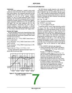
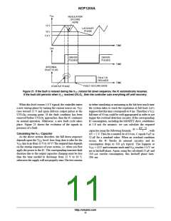
Dynamic Self−Supply
The DSS principle is based on the charge/discharge of the
V
CC
bulk capacitor from a low level up to a higher level. We
can easily describe the current source operation with a bunch
of simple logical equations:
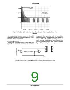
If ICC2 equals 2.3 mA @ T = 25°C, then the power
J
POWER−ON: IF V < VCC THEN Current Source is
ON, no output pulses
CC
H
dissipated (lost) by the IC is simply: 350 x 2.3 m = 805 mW.
For design and reliability reasons, it would be interesting to
reduce this source of wasted power which increases the die
temperature. This can be achieved by using different
methods:
IF V decreasing > VCC THEN Current Source is OFF,
CC
L
output is pulsing
IF V increasing < VCC THEN Current Source is ON,
CC
H
1. Use a MOSFET with lower gate charge Qg
2. Connect pin through a diode (1N4007 typically) to
one of the mains input. The average value on pin 8
output is pulsing
Typical values are: VCC = 12 V, VCC = 10 V
H
L
To better understand the operational principle, Figure 15’s
sketch offers the necessary light:
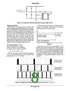
V
MAINS(peak) @ 2
becomes
. Our power
p
contribution example drops to: 223 x 2.3 m = 512
mW. If a resistor is installed between the mains and
the diode, you further force the dissipation to
migrate from the package to the resistor. The
resistor value should account for low−line startups.
V
ripple
= 2 V
UVLO = 12 V
H
V
CC
UVLO = 10 V
L
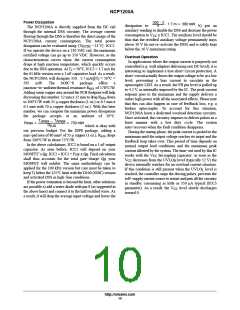
3. Permanently force the V level above VCC with
CC
H
an auxiliary winding. It will automatically
ON
disconnect the internal startup source and the IC
will be fully self−supplied from this winding.
Again, the total power drawn from the mains will
significantly decrease. Make sure the auxiliary
voltage never exceeds the 16 V limit.
Current
Source
OFF
OUTPUT PULSES
10.0 M
30.0 M
50.0 M
70.0 M
90.0 M
Figure 15. The charge/discharge cycle over a
10 mF VCC capacitor
http://onsemi.com
7

 ONSEMI [ ONSEMI ]