NCP1200A
Protecting the Controller Against Negative Spikes
As with any controller built upon a CMOS technology, it
is the designer’s duty to avoid the presence of negative
spikes on sensitive pins. Negative signals have the bad habit
to forward bias the controller substrate and induce erratic
behaviors. Sometimes, the injection can be so strong that
internal parasitic SCRs are triggered, engendering
irremediable damages to the IC if they are a low impedance
fed by its V capacitor and keeps activating the MOSFET
ON and OFF with a peak current limited by Rsense.
CC
Unfortunately, if the quality coefficient Q of the resonating
network formed by Lp and Cbulk is low (e.g. the MOSFET
Rdson + Rsense are small), conditions are met to make the
circuit resonate and thus negatively bias the controller. Since
we are talking about ms pulses, the amount of injected
charge (Q = I x t) immediately latches the controller which
brutally discharges its V capacitor. If this V capacitor
path is offered between V and GND. If the current sense
CC
CC
CC
pin is often the seat of such spurious signals, the
high−voltage pin can also be the source of problems in
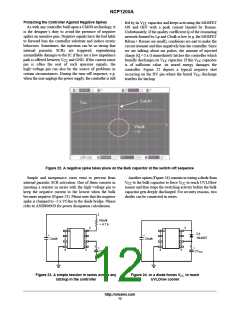
certain circumstances. During the turn−off sequence, e.g.
when the user unplugs the power supply, the controller is still
is of sufficient value, its stored energy damages the
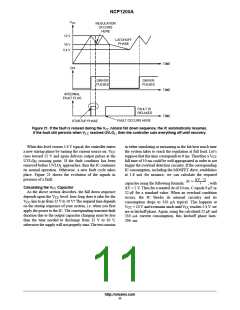
controller. Figure 22 depicts a typical negative shot
occurring on the HV pin where the brutal V discharge
CC
testifies for latchup.
Figure 22. A negative spike takes place on the Bulk capacitor at the switch−off sequence
Simple and inexpensive cures exist to prevent from
internal parasitic SCR activation. One of them consists in
inserting a resistor in series with the high−voltage pin to
keep the negative current to the lowest when the bulk
becomes negative (Figure 23). Please note that the negative
spike is clamped to –2 x Vf due to the diode bridge. Please
refer to AND8069/D for power dissipation calculations.
Another option (Figure 24) consists in wiring a diode from
to the bulk capacitor to force V to reach UVLOlow
sooner and thus stops the switching activity before the bulk
capacitor gets deeply discharged. For security reasons, two
diodes can be connected in series.
V
CC
CC
3
Rbulk
> 4.7 k
2
3
1
2
3
4
8
7
6
5
1
2
3
4
8
7
6
5
D3
1N4007
+
+
Cbulk
Cbulk
1
1
+
CV
+
CV
CC
CC
Figure 23. A simple resistor in series avoids any
latchup in the controller
Figure 24. or a diode forces VCC to reach
UVLOlow sooner
http://onsemi.com
12

 ONSEMI [ ONSEMI ]