NCN8024R
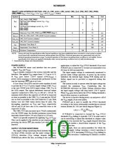
POWER SUPPLY SECTION (V = 3.3 V; V
= 5 V; T
= 25°C; F
= 10 MHz)
DD
DDP
amb
CLKIN
Symbol
Rating
Min
Typ
Max
Unit
V
DC/DC Converter Power Supply,
CRD_V = 5 V
V
DDP
CC
|I | v 70 mA (EMV Conditions)
4.75
4.85
CC
|I | v 70 mA (NDS Conditions)
5.0
5.5
CC
CRD_V = 3 V
CC
|I | v 70 mA
CC
3.0
−
I
I
Inactive Mode
−
−
1
mA
DDP
DC Operating Supply Current, F
= 10 MHz,
⎢ = 0 (CMDVCC = Low)
−
3.0
mA
DDP
CLKIN
Cout
= 33 pF, ⎢I
CRD_CLK
CRD_VCC
I
DC Operating Supply Current,
mA
DDP
CRD_V = 5 V, I
= 70 mA
= 70 mA
−
−
80
80
CC
CRD_VCC
CRD_VCC
CRD_V = 3 V, I
CC
V
Operating Voltage
Inactive Mode 0 Standby Current
Operating Current − F = 10 MHz,
2.7
−
−
−
−
5.5
60
1
V
DD
VDD
VDD
I
I
mA
mA
−
CLK_IN
Cout
= 33 pF, ⎢I
⎢ = 0 (CMDVCC = Low)
CRD_CLK
CRD_VCC
UVLOV
Undervoltage Lockout (UVLO), No External Resistor at Pin PORADJ (Connec-
2.20
50
2.30
100
2.40
180
V
DD
ted to GND), Falling V Level
DD
UVLOHys
UVLO Hysteresis, No External Resistor at Pin PORADJ
(Connected to GND) (Note 4)
mV
PORADJ PIN
V
V
External Rising Threshold Voltage on V for Power On Reset − Pin PORADJ
1.20
1.15
30
1.27
1.20
80
1.34
1.28
100
V
V
PORth+
PORth−
PORHys
DD
External Falling Threshold voltage on V for Power On Reset − Pin PORADJ
DD
V
Hysteresis on V
(pin PORADJ) (Note 4)
mV
ms
PORth
t
Width of Power−On Reset Pulse (Note 4)
No External Resistor on PORADJ
External Resistor on PORADJ
POR
4
4
8
8
12
12
I
IL
Low Level Input Leakage Current, V <0.5 V (Pulldown Current Source)
5
mA
IL
LOW DROP OUT REGULATOR
C
Output Capacitance on card power supply CRD_V (Notes 4 and 5)
80
100 +
220
1200
nF
V
CRD_VCC
CC
CRD_V
Output Card Supply Voltage (including ripple)
CC
CC
3.0 V CRD_V Mode @ I ≤ 70 mA
2.85
4.75
4.60
3.00
5.00
5.00
3.15
5.25
5.25
CC
CC
5.0 V CRD_V Mode @ I ≤ 70 mA with 4.85 V VDDP 5.5 V (NDS)
CC
CC
5.0 V CRD_V Mode @ I ≤ 70 mA with 4.75 V VDDP 5.5 V (EMV)
CC
CC
CRD_V
Current Pulses 40 nAs (t < 400 ns & |I | ≤ 200 mA peak)
V
CC
3.0 V mode / Ripple ≤ 250 mV (2.9 V ≤ VDDP ≤ 5.5 V)
Current Pulses 40 nAs (t < 400 ns & |I | ≤ 200 mA peak)
2.70
4.60
3.00
5.00
3.20
5.25
CC
5.0 V mode / Ripple ≤ 250 mV (4.85 V ≤ VDDP ≤ 5.5 V)
I
Card Supply Current
mA
CRD_VCC
@ CRD_V = 3.0 V
70
70
CC
@ CRD_V = 5.0 V
CC
I
Short−Circuit Current − CRD_V Shorted to Ground
120
150
300
mA
mV
CRD_VCC_SC
CC
DV
Output Card Supply Voltage Ripple Peak−to−Peak − f
200 MHz (Load Transient with 65 mA Peak Current) (Note 4)
= 100 Hz to
CRD_VCC
ripple
CRD_V
Slew Rate on CRD_V Up or Down (Note 4)
0.22
V/ms
CCSR
CC
NOTE: Device will meet the specifications after thermal equilibrium has been established when mounted in a test socket or printed
circuit board with maintained transverse airflow greater than 500 lfpm. Electrical parameters are guaranteed only over the
declared operating temperature range. Functional operation of the device exceeding these conditions is not implied. Device
specification limit values are applied individually under normal operating conditions and not valid simultaneously.
4. Guaranteed by design and characterization
5. These values take into account the tolerance of the cms capacitor used. The allowed values are single or distributed capacitor combination
not exceeding 1.2 mF with 100 nF + 220 nF typical and recommended. It is recommended to use X5R or X7R−type capacitors with very
low ESR (< 100 mW) for optimal performances.
http://onsemi.com
6

 ONSEMI [ ONSEMI ]