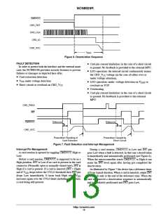
NCN8024R
SMART CARD INTERFACE SECTION, CRD_IO, CRD_AUX1, CRD_AUX2, CRD_CLK, CRD_RST, CRD_PRES,
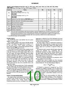
CRD_PRES (V = 3.3 V; V
= 5 V; T
= 25°C; F
= 10 MHz)
DD
DDP
amb
CLKIN
Symbol
Rating
Min
Typ
Max
Unit
CRD_PRES, CRD_PRES
mA
|I
|
High level input leakage current, V = V
IH
IH
DD
CRD_PRES
CRD_PRES
Low level input leakage current, V = 0 V
CRD_PRES
CRD_PRES
3
10
1
|I |
IL
IL
1
10
3
8
T
Debounce Time CRD_PRES and CRD_PRES (Note 7)
CRD_IO, CRD_AUX1, CRD_AUX2 Current Limitation
CRD_CLK Current Limitation
5
−
12
15
ms
mA
mA
mA
ms
debounce
I
−
CRD_IO
CRD_CLK
CRD_RST
I
−
−
70
I
CRD_RST Current Limitation
−
−
20
t
act
Activation Time (Note 7)
30
30
−
−
100
250
−
t
Deactivation Time (Note 7)
−
ms
deact
Temp
Shutdown Temperature
160
°C
SD
NOTE: Device will meet the specifications after thermal equilibrium has been established when mounted in a test socket or printed
circuit board with maintained transverse airflow greater than 500 lfpm. Electrical parameters are guaranteed only over the
declared operating temperature range. Functional operation of the device exceeding these conditions is not implied. Device
specification limit values are applied individually under normal operating conditions and not valid simultaneously.
7. Guaranteed by design and characterization
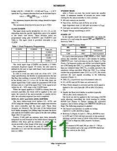
POWER SUPPLY
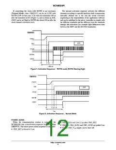
The NCN8024R smart card interface has two power
application, to adjust the V UVLO threshold. If not used
PORADJ pin is connected to Ground (recommended even
if it may be left unconnected).
The input supply voltage is continuously monitored to
prevent under voltage operation. At power up, the system
initializes the internal logic during POR timing and no
further signal can be provided or supported during this
period.
DD
supplies: V and V
.
DD
DDP
V
DD
is usually common to the system controller and the
interface. The applied V ranges from 2.7 V up to 5.5 V.
DD
If V
goes below 2.30 V typical (UVLO
) a
DD
VDD
power−down sequence is automatically performed. In that
case the interrupt (INT) pin is set Low.
A Low Drop−Out (LDO) and low noise regulator is used
to provide the 3 V or 5 V power supply voltage (CRD_V
to the card. VDDP is the LDO’s input voltage. CRD_V is
the LDO output. The typical distributed reservoir output
capacitor connected to CRD_V is 100 nF + 220 nF. To
minimize dI/dt effects the capacitor of 100 nF is connected
as close as possible to the CRD_V ’s pin and the 220 nF
one as close as possible to the card connector C1 pin. Both
feature very low ESR values (lower than 50 mW). The
decoupling capacitors on V
100 nF and 10 mF have also to be connected close to the
respective IC pins.
The CRD_VCC pin can source up to 70 mA continuously
over the VDDP range, the absolute maximum current being
internally limited below 150 mA (Typical at 120 mA).
The system is ready to operate when the input voltage has
)
CC
reached the minimum
V . Considering this, the
DD
NCN8024R will detect an Under−Voltage situation when
the input supply voltage will drop below 2.30 V typical.
CC
When V goes down below the UVLO falling threshold a
CC
DD
deactivation sequence is performed.
The device is inactive during power−on and power−off of
CC
the V supply (8 ms reset pulse).
DD
PORADJ pin is used to modify the UVLO threshold
according to the below relationship considering an external
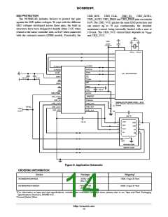
resistor divider R1 / R2 (see block diagram Figure 1):
and V
respectively
DD
DDP
R1 ) R2
UVLO +
VPOR
R2
If PORADJ is connected to Ground the V
UVLO
DD
threshold (V falling) is typically 2.30 V. In some cases it
DD
There’s no specific sequence for applying V or V
.
DD
DDP
can be interesting to adjust this threshold at a higher value
They can be applied to the interface in any sequence. After
powering the device INT pin remains Low until a card is
inserted.
and by the way increase the V supply dropout detection
DD
level which enables a deactivation sequence if the V
voltage is too low.
DD
For example, there are microcontrollers for which the
minimum supply voltage insuring a correct operating is
SUPPLY VOLTAGE MONITORING
The supply voltage monitoring block includes the Power
On Reset (POR) circuitry and the under voltage lockout
higher than 2.70 V, increasing UVLO
(V falling) is
VDD
DD
consequently necessary. Considering for instance a resistor
(UVLO) detection (V
voltage dropout detection).
DD
PORADJ pin allows the user, according to the considered
http://onsemi.com
9

 ONSEMI [ ONSEMI ]