NCL30486B
Application Information
The NCL30486B implements
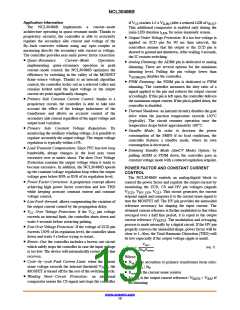
if V reaches 1.5 x V
(after a reduced LEB of t ).
BCS
CS
ILIM
a
current−mode
This additional comparator is enabled only during the
main LEB duration t , for noise immunity reason.
architecture operating in quasi−resonant mode. Thanks to
proprietary circuitry, the controller is able to accurately
regulate the secondary side current and voltage of the
fly−back converter without using any opto−coupler or
measuring directly the secondary side current or voltage.
The controller provides near unity power factor correction
LEB
• Output Under Voltage Protection: If a too low voltage is
applied on ZCD pin for 90 ms time interval, the
controllers assume that the output or the ZCD pin is
shorted to ground and shutdown. After waiting 4 seconds,
the IC restarts switching.
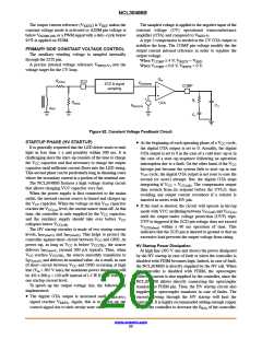
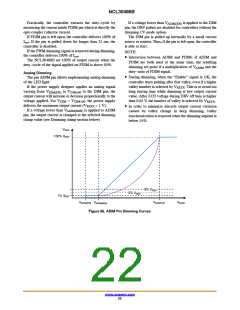
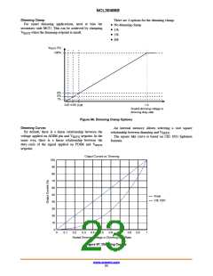
• Analog Dimming: the ADIM pin is dedicated to analog
dimming. There are several options for the minimum
dimming level. Pulling the pin voltage lower than
• Quasi−Resonance
Current−Mode
Operation:
implementing quasi−resonance operation in peak
current−mode control, the NCL30486B optimizes the
efficiency by switching in the valley of the MOSFET
drain−source voltage. Thanks to an internal algorithm
control, the controller locks−out in a selected valley and
remains locked until the input voltage or the output
current set point significantly changes.
V
disables the controller.
ADIM(EN)
• PWM Dimming: the PDIM pin is dedicated to PWM
dimming. The controller measures the duty ratio of a
signal applied to the pin and reduces the output current
accordingly. If this pin is left open, the controller delivers
the maximum output current. If the pin is pulled down, the
controller is disabled.
• Thermal Shutdown: an internal circuitry disables the gate
drive when the junction temperature exceeds 150°C
(typically). The circuit resumes operation once the
temperature drops below approximately 100°C.
• Standby Mode: In order to decrease the power
consumption of the SMPS if no load conditions, the
controller features a standby mode, where its own
consumption is decreased.
• Dimming Standby Mode (dimCV Mode) Option: by
pulling ADIM or PDIM down, the controller goes in
constant voltage mode with a reduced regulation setpoint.
• Primary Side Constant Current Control: thanks to a
proprietary circuit, the controller is able to take into
account the effect of the leakage inductance of the
transformer and allows an accurate control of the
secondary side current regardless of the input voltage and
output load variation.
• Primary Side Constant Voltage Regulation: By
monitoring the auxiliary winding voltage, it is possible to
regulate accurately the output voltage. The output voltage
regulation is typically within 2%.
• Load Transient Compensation: Since PFC has low loop
bandwidth, abrupt changes in the load may cause
excessive over or under−shoot. The slow Over Voltage
Protection contains the output voltage when it tends to
become excessive. In addition, the NCL30486B speeds
up the constant voltage regulation loop when the output
voltage goes below 80% or 85% of its regulation level.
• Power Factor Correction: A proprietary concept allows
achieving high power factor correction and low THD
while keeping accurate constant current and constant
voltage control.
POWER FACTOR AND CONSTANT CURRENT
CONTROL
The NCL30486B embeds an analog/digital block to
control the power factor and regulate the output current by
monitoring the ZCD, CS and HV pin voltages (signals
V
, V
, V ). This circuit generates the current
HV_DIV CS
ZCD
setpoint signal and compares it to the current sense signal to
turn the MOSFET off. The HV pin provides the sinusoidal
reference necessary for shaping the input current. The
obtained current reference is further modulated so that when
averaged over a half line period, it is equal to the output
• Line Feed−forward: allows compensating the variation of
the output current caused by the propagation delay.
• V Over Voltage Protection: if the V pin voltage
CC
CC
exceeds an internal limit, the controller shuts down and
waits 4 seconds before restarting pulsing.
current reference (V
). The modulation and averaging
REFX
process is made internally by a digital circuit. If the HV pin
properly conveys the sinusoidal shape, power factor will be
close to 1. Also, the Total Harmonic Distortion (THD) will
be low especially if the output voltage ripple is small.
• Fast Over Voltage Protection: If the voltage of ZCD pin
exceeds 130% of its regulation level, the controller shuts
down and waits 4 s before trying to restart.
• Brown−Out: the controller includes a brown−out circuit
which safely stops the controller in case the input voltage
is too low. The device will automatically restart if the line
recovers.
VREF
(eq. 1)
IOUT
+
2NspRsense
Where:
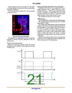
• Cycle−by−cycle Peak Current Limit: when the current
• N is the secondary to primary transformer turns ratio:
sp
sense voltage exceeds the internal threshold V
, the
ILIM
N
• R
• V
= N / N
S P
sp
MOSFET is turned off for the rest of the switching cycle.
• Winding Short−Circuit Protection: an additional
comparator senses the CS signal and stops the controller
is the current sense resistor
sense
is the output current reference: V
= V
if
REFX
REFX
REF
no dimming
www.onsemi.com
19

 ONSEMI [ ONSEMI ]