MT9M021, MT9M031
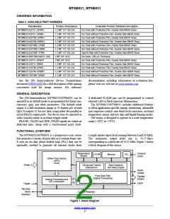
ORDERING INFORMATION
Table 2. AVAILABLE PART NUMBERS
Part Number
Product Description
Orderable Product Attribute Description
MT9M021IA3XTC−DPBR1
MT9M021IA3XTC−DRBR
MT9M021IA3XTM−DPBR1
MT9M021IA3XTM−DRBR1
MT9M021IA3XTMZ−DPBR
MT9M021IA3XTMZ−DRBR
MT9M021IA3XTMZ−TPBR
MT9M031D00STMC24BC1−200
MT9M031I12STC−DPBR1
MT9M031I12STC−DRBR
MT9M031I12STM−DPBR
MT9M031I12STM−DRBR1
MT9M031I12STMZ−DRBR
1.2 MP 1/3″ GS CIS
1.2 MP 1/3″ GS CIS
1.2 MP 1/3″ GS CIS
1.2 MP 1/3″ GS CIS
1.2 MP 1/3″ GS CIS
1.2 MP 1/3″ GS CIS
1.2 MP 1/3″ GS CIS
1 MP 1/6″ SOC
Dry Pack with Protective Film, Double Side BBAR Glass
Dry Pack without Protective Film, Double Side BBAR Glass
Dry Pack with Protective Film, Double Side BBAR Glass
Dry Pack without Protective Film, Double Side BBAR Glass
Dry Pack with Protective Film, Double Side BBAR Glass
Dry Pack without Protective Film, Double Side BBAR Glass
Tape & Reel with Protective Film, Double Side BBAR Glass
Die Sales, 200 mm Thickness
1 MP 1/6″ SOC
Dry Pack with Protective Film, Double Side BBAR Glass
Dry Pack without Protective Film, Double Side BBAR Glass
Dry Pack with Protective Film, Double Side BBAR Glass
Dry Pack without Protective Film, Double Side BBAR Glass
Dry Pack without Protective Film, Double Side BBAR Glass
1.2 MP 1/3″ GS CIS
1.2 MP 1/3″ GS CIS
1.2 MP 1/3″ GS CIS
1.2 MP 1/3″ GS CIS
See the ON Semiconductor Device Nomenclature
document (TND310/D) for a full description of the naming
convention used for image sensors. For reference
documentation, including information on evaluation kits,
please visit our web site at www.onsemi.com.
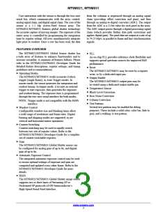
GENERAL DESCRIPTION
The ON Semiconductor MT9M021/MT9M031 can be
operated in its default mode or programmed for frame size,
exposure, gain, and other parameters. The default mode
output is a full-resolution image at 45 frames per second
(fps). It outputs 12-bit raw data, using either the parallel or
serial (HiSPi) output ports. The device may be operated in
video (master) mode or in frame trigger mode.
A dedicated FLASH pin can be programmed to control
external LED or flash exposure illumination.
The MT9M021/MT9M031 includes additional features
to allow application-specific tuning: windowing, adjustable
auto-exposure control, auto black level correction, on-board
temperature sensor, and row skip and digital binning modes.
The sensor is designed to operate in a wide temperature
range (–30°C to +70°C).
FRAME_VALID and LINE_VALID signals are output on
dedicated pins, along with a synchronized pixel clock.
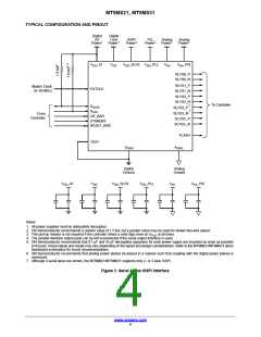
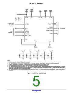
FUNCTIONAL OVERVIEW
The MT9M021/MT9M031 is a progressive-scan sensor
that generates a stream of pixel data at a constant frame rate.
It uses an on-chip, phase-locked loop (PLL) that can be
optionally enabled to generate all internal clocks from
a single master input clock running between 6 and 50 MHz.
The maximum output pixel rate is 74.25 Mp/s,
corresponding to a clock rate of 74.25 MHz. Figure 1 shows
a block diagram of the sensor.
Temperature
Sensor
External
Clock
OTPM
Memory
PLL
Active Pixel Sensor
(APS)
Array
Power
Timing and Control
(Sequencer)
Auto Exposure
and Stats Engine
Serial
Output
Pixel Data Path
(Signal Processing)
Parallel
Output
Analog Processing and
A/D Conversion
Flash
Trigger
Two-wire
Serial
Control Registers
Interface
Figure 1. Block Diagram
www.onsemi.com
2

 ONSEMI [ ONSEMI ]