MC44603
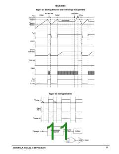
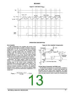
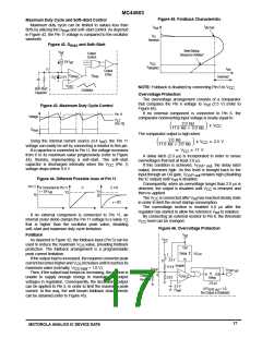
Figure 31. Soft–Start & D
max
V
ref
V
+ 1.6 V
CSS
Internal Clamp
Soft–Start
External Clamp
V
3.6 V
CT
V
low 1.6 V
CT
V
OSC
Output
(Pin 3)
OPERATING DESCRIPTION
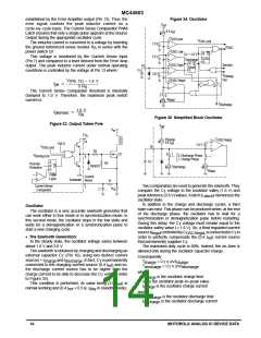
Error Amplifier
Figure 32. Error Amplifier Compensation
+
A fully compensated Error Amplifier with access to the
inverting input and output is provided. It features a typical dc
voltage gain of 70 dB. The noninverting input is internally
biased at 2.5 V and is not pinned out. The converter output
voltage is typically divided down and monitored by the
inverting input. The maximum input bias current with the
inverting input at 2.5 V is –2.0 µA. This can cause an output
voltage error that is equal to the product of the input bias
current and the equivalent input divider source resistance.
The Error Amp output (Pin 13) is provided for external loop
compensation. The output voltage is offset by two diode
drops (≈ 1.4 V) and divided by three before it connects to the
inverting input of the Current Sense Comparator. This
guarantees that no drive pulses appear at the Output (Pin 3)
1.0 mA
Compensation
Error
Amplifier
13
R
FB
R
f
2R
C
2.5 V
f
14
R
Voltage
Feedback
Input
Current Sense
Comparator
5
Foldback
Input
Gnd
4
From Power Supply Output
R2
R1
when Pin 13 is at its lowest state (V ). The Error Amp
OL
minimum feedback resistance is limited by the amplifier’s
minimum source current (0.2 mA) and the required output
Current Sense Comparator and PWM Latch
The MC44603 can operate as a current mode controller or
as a voltage mode controller. In current mode operation, the
MC44603 uses the current sense comparator. The output
switch conduction is initiated by the oscillator and terminated
when the peak inductor current reaches the threshold level
voltage (V
OH
clamp level:
) to reach the current sense comparator’s 1.0 V
3.0 (1.0 V) 1.4 V
R
22 k
f(min)
0.2 mA
13
MOTOROLA ANALOG IC DEVICE DATA

 ONSEMI [ ONSEMI ]