MC44603
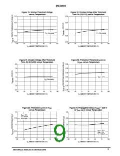
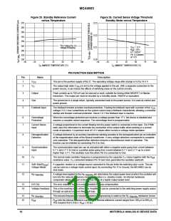
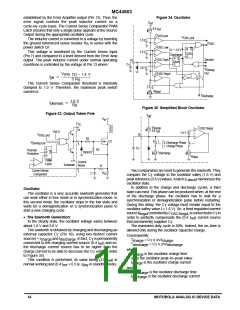
Figure 25. Standby Reference Current
versus Temperature
Figure 26. Current Sense Voltage Threshold
Standby Mode versus Temperature
270
265
260
0.33
0.32
0.31
0.30
255
250
V
R P Stdby (Pin 12)
Voltage Increasing
245
V
R
C
= 12 V
= 10 k
= 820 pF
CC
ref
T
240
235
230
Pin 12 Clamped
at 1.0 V
–50
–25
0
25
50
75
100
–50
–25
0
25
50
75
100
T , AMBIENT TEMPERATURE (
°C)
T , AMBIENT TEMPERATURE (°C)
A
A
PIN FUNCTION DESCRIPTION
Pin
1
Name
Description
This pin is the positive supply of the IC. The operating voltage range after startup is 9.0 to 14.5 V.
The output high state (V ) is set by the voltage applied to this pin. With a separate connection to the
V
CC
2
V
C
OH
power source, it can reduce the effects of switching noise on the control circuitry.
3
4
5
Output
Peak currents up to 750 mA can be sourced or sunk, suitable for driving either MOSFET or Bipolar
transistors. This output pin must be shunted by a Schottky diode, 1N5819 or equivalent.
Gnd
The ground pin is a single return, typically connected back to the power source; it is used as control and
power ground.
Foldback Input
The foldback function provides overload protection. Feeding the foldback input with a portion of the V
CC
voltage (1.0 V max) establishes on the system control loop a foldback characteristic allowing a smoother
startup and sharper overload protection. Above 1.0 V the foldback input is inactive.
6
7
Overvoltage
Protection
When the overvoltage protection pin receives a voltage greater than 17 V, the device is disabled and
requires a complete restart sequence. The overvoltage level is programmable.
Current Sense
Input
A voltage proportional to the current flowing into the power switch is connected to this input. The PWM
latch uses this information to terminate the conduction of the output buffer when working in a current
mode of operation. A maximum level of 1.0 V allows either current or voltage mode operation.
8
9
Demagnetization
Detection
A voltage delivered by an auxiliary transformer winding provides to the demagnetization pin an indication
of the magnetization state of the flyback transformer. A zero voltage detection corresponds to complete
core saturation. The demagnetization detection ensures a discontinuous mode of operation. This
function can be inhibited by connecting Pin 8 to Gnd.
Synchronization
Input
The synchronization input pin can be activated with either a negative pulse going from a level between
0.7 V and 3.7 V to Gnd or a positive pulse going from a level between 0.7 V and 3.7 V up to a level
higher than 3.7 V. The oscillator runs free when Pin 9 is connected to Gnd.
10
11
C
The normal mode oscillator frequency is programmed by the capacitor C choice together with the R
ref
T
T
resistance value. C , connected between Pin 10 and Gnd, generates the oscillator sawtooth.
T
Soft–Start/D
max
Voltage–Mode
/
A capacitor, resistor or a voltage source connected to this pin limits the switching duty–cycle. This pin
can be used as a voltage mode control input. By connecting Pin 11 to Ground, the MC44603 can be
shut down.
12
R
A voltage level applied to the R pin determines the output power level at which the oscillator will
P Standby
turn into the reduced frequency mode of operation (i.e. standby mode). An internal hysteresis
comparator allows to return in the normal mode at a higher output power level.
P Standby
13
14
E/A Out
Voltage Feedback
The error amplifier output is made available for loop compensation.
This is the inverting input of the Error Amplifier. It can be connected to the switching power supply output
through an optical (or other) feedback loop.
15
16
R
R
The reduced frequency or standby frequency programming is made by the R
resistance choice.
sets the internal reference current. The internal reference current ranges from 100 µA to 500 µA.
F Standby
ref
F Standby
R
ref
This requires that 5.0 kΩ ≤ R ≤ 25 kΩ.
ref
10
MOTOROLA ANALOG IC DEVICE DATA

 ONSEMI [ ONSEMI ]