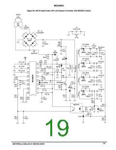
MC44603
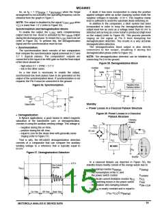
So, as f = 1 /(T
charge
+ T
) when the Regul
A diode D has been incorporated to clamp the positive
applied voltages while an active clamping system limits the
negative voltages to typically –0.33 V. This negative clamp
level is sufficient to avoid the substrate diode switching on.
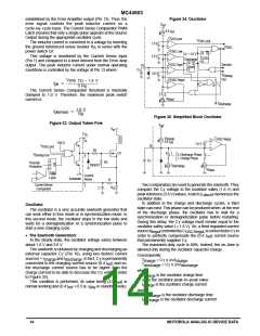
In addition to the comparator, a latch system has been
incorporated in order to keep the demagnetization block
output level low as soon as a voltage lower than 65 mV is
detected and as long as a new restart is produced (high level
on the output) (refer to Figure 38). This process prevents
ringing on the signal at Pin 8 from disrupting the
demagnetization detection. This results in a very accurate
demagnetization detection.
S
discharge
arrangement is not activated, the operating frequency can be
obtained from the graph in Figure 1.
NOTE: The output is disabled by the signal V
when
OSC prot
V
is lower than 1.0 V (refer to Figure 30).
CT
Synchronization and Demagnetization Blocks
To enable the output, the L latch complementary
OSC
output must be low. Reset is activated by the L
during the discharge phase. To restart, the L
(refer to Figure 34). To perform this, the demagnetization
signal and the synchronization must be low.
output
disch
has to be set
OSC
The demagnetization block output is also directly
connected to the output, disabling it during the
demagnetization phase (refer to Figure 33).
• Synchronization:
The synchronization block consists of two comparators
that compare the synchronization signal (external) to 0.7 and
3.7 V (typical values). The comparators’ outputs are
connected to the input of an AND gate so that the final output
of the block should be :
NOTE: The demagnetization detection can be inhibited by
connecting Pin 8 to the ground.
Figure 38. Demagnetization Block
– high when 0.7 < SYNC < 3.7 V
– low in the other cases.
Oscillator
Output
R
Q
Buffer
As a low level is necessary to enable the output,
synchronized low level pulses have to be generated on the
output of the synchronization block. If synchronization is not
required, the Pin 9 must be connected to the ground.
Demag
S
V
CC
Negative Active
Clamping System
Figure 36. Synchronization
V
Demag Out
3.7 V
8
C Dem
65 mV
Oscillator
Sync
9
D
Standby
Output Buffer
0.7 V
• Power Losses in a Classical Flyback Structure
Figure 39. Power Losses in a Classical
Flyback Structure
• Demagnetization:
In flyback applications, a good means to detect magnetic
saturation of the transformer core, or demagnetization,
consists in using the auxiliary winding voltage. This voltage is:
Clamping
Network
V
in
R
ICL
– negative during the on–time,
– positive during the off–time,
+
+
AC Line
– equal to zero for the dead–time with generally some
– ringing (refer to Figure 37).
R
startup
That is why, the MC44603 demagnetization detection
consists of a comparator that can compare the auxiliary
winding voltage to a reference that is typically equal to
65 mV.
V
CC
MC44603
R
S
Figure 37. Demagnetization Detection
Snubber
In a classical flyback (as depicted in Figure 39), the
standby losses mainly consist of the energy waste due to:
0.75 V
Zero Current
Detection
V
Pin 8
– the startup resistor R
startup
P
startup
– the consumption of the IC and
– the power switch control
P
control
65 mV
– the inrush current limitation resistor R
P
ICL
ICL
– the switching losses in the power switch
– the snubber and clamping network
P
SW
–0.33 V
P
SN–CLN
P
is nearly constant and is equal to:
startup
On–Time
Off–Time
Dead–Time
2
R
startup
(V –V
in CC
)
15
MOTOROLA ANALOG IC DEVICE DATA

 ONSEMI [ ONSEMI ]