MC44603
Figure 45. Foldback Characteristic
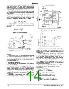
Maximum Duty Cycle and Soft–Start Control
Maximum duty cycle can be limited to values less than
80% by utilizing the D and soft–start control. As depicted
in Figure 42, the Pin 11 voltage is compared to the oscillator
sawtooth.
I
V
pk max
out
max
V
O
Nominal
Figure 42. D
and Soft–Start
max
New Startup
Sequence Initiated
V
ref
Output
Control
0.4 I
ref
V
CC
disable2
V
I
11
out
Output
Drive
C
D
Dmax
max
Overload
D
2.4 V
Z
V
OSC
NOTE: Foldback is disabled by connecting Pin 5 to V
.
CC
Soft–Start
Capacitor
Oscillator
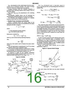
Overvoltage Protection
The overvoltage arrangement consists of a comparator
that compares the Pin 6 voltage to V
Figure 46).
(2.5 V) (refer to
ref
Figure 43. Maximum Duty Cycle Control
If no external component is connected to Pin 6, the
comparator noninverting input voltage is nearly equal to:
Pin 11
Voltage
V
CT
(Pin 10)
2.0 k
11.6 k
x V
CC
2.0 k
D
max
The comparator output is high when:
2.0 k
11.6 k
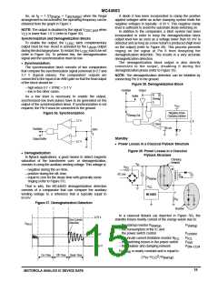
Using the internal current source (0.4 I ), the Pin 11
ref
x V
2.5 V
CC
2.0 k
voltage can easily be set by connecting a resistor to this pin.
If a capacitor is connected to Pin 11, the voltage increases
from 0 to its maximum value progressively (refer to Figure
44), thereby, implementing a soft–start. The soft–start
V
17 V
CC
A delay latch (2.0 µs) is incorporated in order to sense
overvoltages that last at least 2.0 µs.
If this condition is achieved, V , the delay latch
output, becomes high. As this level is brought back to the
input through an OR gate, V remains high (disabling
capacitor is discharged internally when the V
voltage drops below 9.0 V.
(Pin 1)
CC
OVP out
OVP out
Figure 44. Different Possible Uses of Pin 11
the IC output) until V is disabled.
ref
Consequently, when an overvoltage longer than 2.0 µs is
Pin 11
RI
R Connected to Pin 11
I = 0.4 I
C
C // R
detected, the output is disabled until V
then re–applied.
is connected after V has reached steady state
in order to limit the circuit startup consumption.
is removed and
CC
V
RI
V
Z
ref
Z
The V
CC
ref
τ
= RC
The overvoltage section is enabled 5.0 µs after the
regulator has started to allow the reference V to stabilize.
ref
If no external component is connected to Pin 11, an
internal zener diode clamps the Pin 11 voltage to a value V
that is higher than the oscillator peak value, disabling
soft–start and maximum duty cycle limitation.
By connecting an external resistor to Pin 6, the threshold
Z
V
level can be changed.
CC
Figure 46. Overvoltage Protection
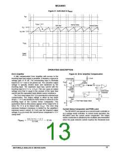
Foldback
V
ref
V
As depicted in Fgure 32, the foldback input (Pin 5) can be
CC
used to reduce the maximum V
protection. The foldback arrangement is a programmable
peak current limitation.
value, providing foldback
CS
Out
Delay
In
5.0 µs
τ
T
If the output load is increased, the required converter peak
2.5 V
0
current becomes higher and V
increases until it reaches its
CS
Enable
11.6 k
maximum value (normally, V
= 1.0 V).
CS max
V
OVP
6
V
OVP out
Then, if the output load keeps on increasing, the system is
unable to supply enough energy to maintain the output
voltages in regulation. Consequently, the decreasing output
can be applied to Pin 5, in order to limit the maximum peak
current. In this way, the well known foldback characteristic
can be obtained (refer to Figure 45).
τ
In
Out
C
External
Resistor
OVLO
2.0 k
Delay
2.0 µs
2.5 V
(If V
= 1.0,
OVP out
(V
)
ref
the Output is Disabled)
17
MOTOROLA ANALOG IC DEVICE DATA

 ONSEMI [ ONSEMI ]