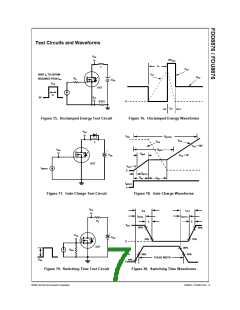
Test Circuits and Waveforms
V
DS
BV
DSS
t
P
L
V
DS
I
VARY t TO OBTAIN
P
AS
+
-
V
DD
R
REQUIRED PEAK I
G
AS
V
DD
V
GS
DUT
t
P
I
0V
AS
0
0.01Ω
t
AV
Figure 15. Unclamped Energy Test Circuit
Figure 16. Unclamped Energy Waveforms
V
DS
V
Q
DD
g(TOT)
V
GS
V
L
DS
V
= 10V
GS
Q
V
g(5)
GS
+
-
Q
gs2
V
V
= 5V
DD
GS
DUT
V
= 1V
GS
I
g(REF)
0
Q
g(TH)
Q
Q
gs
gd
I
g(REF)
0
Figure 17. Gate Charge Test Circuit
Figure 18. Gate Charge Waveforms
V
DS
t
t
ON
OFF
t
d(OFF)
t
d(ON)
R
L
t
t
f
r
V
DS
90%
90%
+
-
V
GS
V
DD
10%
10%
0
DUT
90%
50%
R
GS
V
GS
50%
PULSE WIDTH
V
10%
GS
0
Figure 19. Switching Time Test Circuit
Figure 20. Switching Time Waveforms
©2008 Fairchild Semiconductor Corporation
FDD8876 / FDU8876 Rev. 1.2

 ONSEMI [ ONSEMI ]