Package Marking and Ordering Information
Device Marking
Device
Package
Reel Size
Tape Width
Quantity
FDB3632
FDB3632-F085
TO-263AB
330mm
24mm
800 units
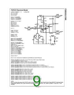
Electrical Characteristics TC = 25°C unless otherwise noted
Symbol
Parameter
Test Conditions
Min
Typ
Max
Units
Off Characteristics
BVDSS
Drain to Source Breakdown Voltage
Zero Gate Voltage Drain Current
Gate to Source Leakage Current
ID = 250µA, VGS = 0V
100
-
-
-
-
-
V
V
DS = 80V
-
-
-
1
IDSS
µA
nA
VGS = 0V
TC= 150oC
250
±100
IGSS
VGS = ±20V
On Characteristics
VGS(TH)
Gate to Source Threshold Voltage
VGS = VDS, ID = 250µA
ID=80A, VGS=10V
ID=80A, VGS=10V, TC=175oC
2
-
-
4
V
0.0075 0.009
0.018 0.022
rDS(ON)
Drain to Source On Resistance
Ω
-
Dynamic Characteristics
CISS
Input Capacitance
-
-
-
-
-
-
-
-
6000
820
200
84
-
pF
pF
pF
nC
nC
nC
nC
nC
VDS = 25V, VGS = 0V,
f = 1MHz
COSS
CRSS
Qg(TOT)
Qg(TH)
Qgs
Output Capacitance
-
Reverse Transfer Capacitance
Total Gate Charge at 10V
Threshold Gate Charge
-
110
14
-
VGS = 0V to 10V
VGS = 0V to 2V
11
VDD = 50V
ID = 80A
Gate to Source Gate Charge
Gate Charge Threshold to Plateau
Gate to Drain “Miller” Charge
30
Ig = 1.0mA
Qgs2
20
-
Qgd
20
-
Resistive Switching Characteristics (VGS = 10V)
tON
td(ON)
tr
Turn-On Time
Turn-On Delay Time
Rise Time
-
-
-
-
-
-
-
102
ns
ns
ns
ns
ns
ns
30
39
96
46
-
-
-
VDD = 50V, ID = 80A
GS = 10V, RGS = 3.6Ω
V
td(OFF)
tf
Turn-Off Delay Time
Fall Time
-
-
tOFF
Turn-Off Time
213
Drain-Source Diode Characteristics
I
I
SD = 80A
SD = 40A
-
-
-
-
-
-
-
-
1.25
1.0
64
V
V
VSD
Source to Drain Diode Voltage
trr
Reverse Recovery Time
ISD = 75A, dISD/dt= 100A/µs
ISD = 75A, dISD/dt= 100A/µs
ns
nC
QRR
Reverse Recovered Charge
120
Notes:
1: Starting T = 25°C, L = 0.12mH, I = 75A.
J
AS
2: Pulse Width = 100s
www.onsemi.com
2

 ONSEMI [ ONSEMI ]