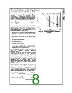
Thermal Resistance vs. Mounting Pad Area
The maximum rated junction temperature, TJM, and the
80
thermal resistance of the heat dissipating path determines
the maximum allowable device power dissipation, PDM, in an
R
= 26.51+ 19.84/(0.262+Area) EQ.2
θJA
R
= 26.51+ 128/(1.69+Area) EQ.3
θJA
application.
Therefore the application’s ambient
temperature, TA (oC), and thermal resistance RθJA (oC/W)
must be reviewed to ensure that TJM is never exceeded.
Equation 1 mathematically represents the relationship and
serves as the basis for establishing the rating of the part.
60
40
20
(T
– T )
A
JM
(EQ. 1)
P
= -----------------------------
DM
RθJA
In using surface mount devices such as the TO-263
package, the environment in which it is applied will have a
significant influence on the part’s current and maximum
power dissipation ratings. Precise determination of PDM is
complex and influenced by many factors:
0.1
(0.645)
1
10
(6.45)
(64.5)
2
2
AREA, TOP COPPER AREA in (cm )
Figure 21. Thermal Resistance vs Mounting
Pad Area
1. Mounting pad area onto which the device is attached and
whether there is copper on one side or both sides of the
board.
2. The number of copper layers and the thickness of the
board.
3. The use of external heat sinks.
4. The use of thermal vias.
5. Air flow and board orientation.
6. For non steady state applications, the pulse width, the
duty cycle and the transient thermal response of the part,
the board and the environment they are in.
ON Semiconductor provides thermal information to
assist
the
designer’s
preliminary
application
evaluation. Figure 21
defines the RθJA for the device as a function of the top
copper (component side) area. This is for a horizontally
positioned FR-4 board with 1oz copper after 1000 seconds
of steady state power with no air flow. This graph provides
the necessary information for calculation of the steady state
junction temperature or power dissipation. Pulse
applications can be evaluated using the ON
Semiconductor device Spice thermal model or manually
utilizing the normalized maximum transient thermal
impedance curve.
Thermal resistances corresponding to other copper areas
can be obtained from Figure 21 or by calculation using
Equation 2 or 3. Equation 2 is used for copper area defined
in inches square and equation 3 is for area in centimeters
square. The area, in square inches or square centimeters is
the top copper area including the gate and source pads.
19.84
(0.262 + Area)
R
= 26.51 + ------------------------------------
(EQ. 2)
θJA
Area in Inches Squared
128
(1.69 + Area)
R
= 26.51 + ---------------------------------
(EQ. 3)
θJA
Area in Centimeters Squared
www.onsemi.com
7

 ONSEMI [ ONSEMI ]