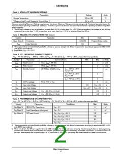
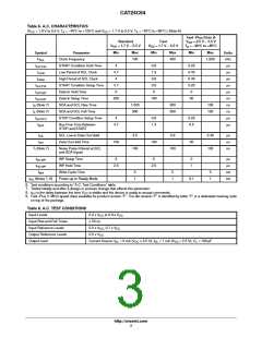
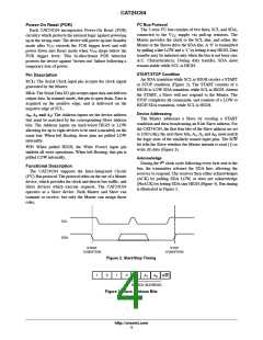
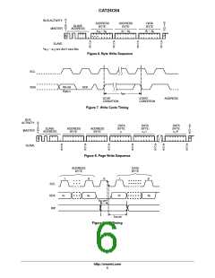
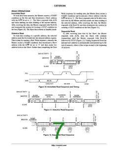
CAT24C64
I2C Bus Protocol
The 2-wire I C bus consists of two lines, SCL and SDA,
connected to the V supply via pull-up resistors. The
Master provides the clock to the SCL line, and either the
Master or the Slaves drive the SDA line. A ‘0’ is transmitted
by pulling a line LOW and a ‘1’ by letting it stay HIGH. Data
transfer may be initiated only when the bus is not busy (see
A.C. Characteristics). During data transfer, SDA must
remain stable while SCL is HIGH.
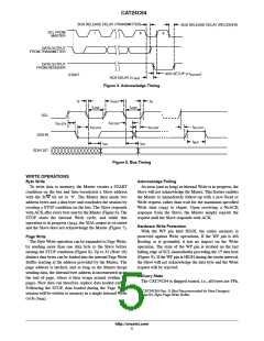
Power-On Reset (POR)
2
Each CAT24C64 incorporates Power-On Reset (POR)
circuitry which protects the internal logic against powering
up in the wrong state. The device will power up into Standby
CC
mode after V exceeds the POR trigger level and will
CC
power down into Reset mode when V drops below the
CC
POR trigger level. This bi-directional POR behavior
protects the device against ‘brown-out’ failure following a
temporary loss of power.
START/STOP Condition
Pin Description
An SDA transition while SCL is HIGH creates a START
or STOP condition (Figure 2). The START consists of a
HIGH to LOW SDA transition, while SCL is HIGH. Absent
the START, a Slave will not respond to the Master. The
STOP completes all commands, and consists of a LOW to
HIGH SDA transition, while SCL is HIGH.
SCL: The Serial Clock input pin accepts the clock signal
generated by the Master.
SDA: The Serial Data I/O pin accepts input data and delivers
output data. In transmit mode, this pin is open drain. Data is
acquired on the positive edge, and is delivered on the
negative edge of SCL.
Device Addressing
A , A and A : The Address inputs set the device address
0
1
2
The Master addresses a Slave by creating a START
condition and then broadcasting an 8-bit Slave address. For
the CAT24C64, the first four bits of the Slave address are set
that must be matched by the corresponding Slave address
bits. The Address inputs are hard-wired HIGH or LOW
allowing for up to eight devices to be used (cascaded) on the
same bus. When left floating, these pins are pulled LOW
internally.
to 1010 (Ah); the next three bits, A , A and A , must match
2
1
0
the logic state of the similarly named input pins. The R/W
bit tells the Slave whether the Master intends to read (1) or
write (0) data (Figure 3).
WP: When pulled HIGH, the Write Protect input pin
inhibits all write operations. When left floating, this pin is
pulled LOW internally.
Acknowledge
During the 9 clock cycle following every byte sent to the
th
Functional Description
bus, the transmitter releases the SDA line, allowing the
receiver to respond. The receiver then either acknowledges
(ACK) by pulling SDA LOW, or does not acknowledge
(NoACK) by letting SDA stay HIGH (Figure 4). Bus timing
is illustrated in Figure 5.
The CAT24C64 supports the Inter-Integrated Circuit
2
(I C) Bus protocol. The protocol relies on the use of a Master
device, which provides the clock and directs bus traffic, and
Slave devices which execute requests. The CAT24C64
operates as a Slave device. Both Master and Slave can
transmit or receive, but only the Master can assign those
roles.
SCL
SDA
START
CONDITION
STOP
CONDITION
Figure 2. Start/Stop Timing
1
0
1
0
A
2
A
1
A
0
R/W
DEVICE ADDRESS
Figure 3. Slave Address Bits
http://onsemi.com
4

 ONSEMI [ ONSEMI ]