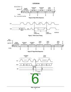
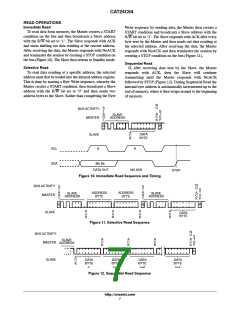
CAT24C64
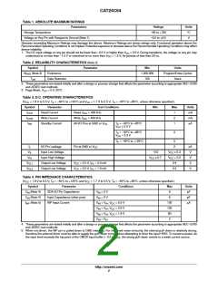
Table 5. A.C. CHARACTERISTICS
(V = 1.8 V to 5.5 V, T = −40°C to +125°C and V = 1.7 V to 5.5 V, T = −40°C to +85°C.) (Note 6)
CC
A
CC
A
Fast−Plus (Note 9)
= 2.5 V − 5.5 V
Standard
= 1.7 V − 5.5 V
Fast
= 1.7 V − 5.5 V
V
CC
V
CC
V
T
= −405C to +855C
CC
A
Min
Max
Min
Max
Min
Max
Symbol
Parameter
Units
kHz
ms
F
SCL
Clock Frequency
100
400
1,000
t
START Condition Hold Time
Low Period of SCL Clock
High Period of SCL Clock
START Condition Setup Time
Data In Hold Time
4
4.7
4
0.6
1.3
0.6
0.6
0
0.25
0.45
0.40
0.25
0
HD:STA
t
ms
LOW
t
ms
HIGH
t
4.7
0
ms
SU:STA
HD:DAT
t
ms
t
Data In Setup Time
250
100
50
ns
SU:DAT
t
(Note 7)
SDA and SCL Rise Time
SDA and SCL Fall Time
STOP Condition Setup Time
1,000
300
300
300
100
100
ns
R
t (Note 7)
ns
F
t
4
0.6
1.3
0.25
0.5
ms
SU:STO
t
Bus Free Time Between
STOP and START
4.7
ms
BUF
t
SCL Low to Data Out Valid
Data Out Hold Time
3.5
0.9
0.40
100
ms
ns
ns
AA
t
100
100
50
DH
T (Note 7)
Noise Pulse Filtered at SCL
and SDA Inputs
100
100
i
t
WP Setup Time
0
0
0
1
ms
ms
SU:WP
t
WP Hold Time
2.5
2.5
HD:WP
t
Write Cycle Time
Power-up to Ready Mode
5
1
5
1
5
1
ms
ms
WR
t
(Notes 7, 8)
0.1
PU
6. Test conditions according to “A.C. Test Conditions” table.
7. Tested initially and after a design or process change that affects this parameter.
8. t is the delay between the time V is stable and the device is ready to accept commands.
PU
CC
9. Fast−Plus (1 MHz) speed class available for product revision “F”. The die revision “F” is identified by letter “F” or a dedicated marking code
on top of the package.
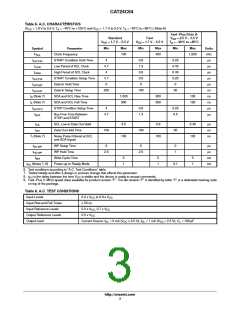
Table 6. A.C. TEST CONDITIONS
Input Levels
0.2 x V to 0.8 x V
CC
CC
Input Rise and Fall Times
Input Reference Levels
Output Reference Levels
Output Load
≤ 50 ns
0.3 x V , 0.7 x V
CC
CC
0.5 x V
CC
Current Source: I = 3 mA (V ≥ 2.5 V); I = 1 mA (V < 2.5 V); C = 100 pF
OL
CC
OL
CC
L
http://onsemi.com
3

 ONSEMI [ ONSEMI ]