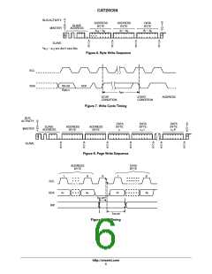
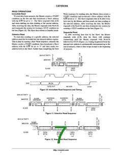
CAT24C64
Table 1. ABSOLUTE MAXIMUM RATINGS
Parameters
Ratings
Units
°C
Storage Temperature
–65 to +150
–0.5 to +6.5
Voltage on Any Pin with Respect to Ground (Note 1)
V
Stresses exceeding Maximum Ratings may damage the device. Maximum Ratings are stress ratings only. Functional operation above the
Recommended Operating Conditions is not implied. Extended exposure to stresses above the Recommended Operating Conditions may affect
device reliability.
1. The DC input voltage on any pin should not be lower than −0.5 V or higher than V + 0.5 V. During transitions, the voltage on any pin may
CC
undershoot to no less than −1.5 V or overshoot to no more than V + 1.5 V, for periods of less than 20 ns.
CC
Table 2. RELIABILITY CHARACTERISTICS (Note 2)
Symbol
(Note 3)
Parameter
Min
1,000,000
100
Units
Program/Erase Cycles
Years
N
Endurance
END
T
DR
Data Retention
2. These parameters are tested initially and after a design or process change that affects the parameter according to appropriate AEC−Q100
and JEDEC test methods.
3. Page Mode, V = 5 V, 25°C.
CC
Table 3. D.C. OPERATING CHARACTERISTICS
(V = 1.8 V to 5.5 V, T = −40°C to +125°C and V = 1.7 V to 5.5 V, T = −40°C to +85°C, unless otherwise specified.)
CC
A
CC
A
Symbol
Parameter
Test Conditions
Min
Max
Units
mA
I
Read Current
Read, f
= 400 kHz
1
2
1
CCR
SCL
I
Write Current
Write, f
= 400 kHz
mA
CCW
SCL
I
SB
Standby Current
All I/O Pins at GND or V
T = −40°C to +85°C
CC
mA
CC
A
V
≤ 3.3 V
T = −40°C to +85°C
CC
3
A
V
> 3.3 V
T = −40°C to +125°C
A
5
2
I
I/O Pin Leakage
Pin at GND or V
mA
V
L
CC
V
Input Low Voltage
Input High Voltage
Output Low Voltage
Output Low Voltage
−0.5
V
x 0.3
IL
CC
V
V
x 0.7
V
CC
+ 0.5
V
IH
CC
V
V
V
< 2.5 V, I = 3.0 mA
0.4
0.2
V
OL1
OL2
CC
OL
V
< 2.5 V, I = 1.0 mA
V
CC
OL
Table 4. PIN IMPEDANCE CHARACTERISTICS
(V = 1.8 V to 5.5 V, T = −40°C to +125°C and V = 1.7 V to 5.5 V, T = −40°C to +85°C, unless otherwise specified.)
CC
A
CC
A
Symbol
Parameter
Conditions
Max
8
Units
pF
C
C
(Note 4)
(Note 4)
(Note 5)
SDA I/O Pin Capacitance
Input Capacitance (other pins)
WP Input Current
V
IN
V
IN
V
IN
V
IN
V
IN
V
IN
= 0 V
= 0 V
IN
IN
6
pF
I
< V , V = 5.5 V
130
120
80
2
mA
WP
IH
CC
< V , V = 3.3 V
IH
CC
< V , V = 1.8 V
IH
IH
CC
> V
4. These parameters are tested initially and after a design or process change that affects the parameter according to appropriate AEC−Q100
and JEDEC test methods.
5. When not driven, the WP pin is pulled down to GND internally. For improved noise immunity, the internal pull−down is relatively strong;
therefore the external driver must be able to supply the pull−down current when attempting to drive the input HIGH. To conserve power, as
the input level exceeds the trip point of the CMOS input buffer (~ 0.5 x V ), the strong pull−down reverts to a weak current source.
CC
http://onsemi.com
2

 ONSEMI [ ONSEMI ]