8TH B
T
ACK
CAT1021, CAT1022, CAT1023
EMBEDDED EEPROM OPERATON
The CAT1021/22/23 feature a 2−kbit embedded serial
EEPROM that supports the I C Bus data transmission
2. During a data transfer, the data line must remain
stable whenever the clock line is high. Any
2
protocol. This Inter−Integrated Circuit Bus protocol defines
any device that sends data to the bus to be a transmitter and
any device receiving data to be a receiver. The transfer is
controlled by the Master device which generates the serial
clock and all START and STOP conditions for bus access.
Both the Master device and Slave device can operate as
either transmitter or receiver, but the Master device controls
which mode is activated.
changes in the data line while the clock line is high
will be interpreted as a START or STOP condition.
Start Condition
The START Condition precedes all commands to the
device, and is defined as a HIGH to LOW transition of SDA
when SCL is HIGH. The CAT1021/22/23 monitor the SDA
and SCL lines and will not respond until this condition is
met.
I2C Bus Protocol
The features of the I C bus protocol are defined as
Stop Condition
2
A LOW to HIGH transition of SDA when SCL is HIGH
determines the STOP condition. All operations must end
with a STOP condition.
follows:
1. Data transfer may be initiated only when the bus is
not busy.
DEVICE ADDRESSING
The Master begins a transmission by sending a START
condition. The Master sends the address of the particular
slave device it is requesting. The four most significant bits
of the 8−bit slave address are programmable in metal and the
default is 1010.
The last bit of the slave address specifies whether a Read
or Write operation is to be performed. When this bit is set to
1, a Read operation is selected, and when set to 0, a Write
operation is selected.
After the Master sends a START condition and the slave
address byte, the CAT1021/22/23 monitors the bus and
responds with an acknowledge (on the SDA line) when its
address matches the transmitted slave address. The
CAT1021/22/23 then perform a Read or Write operation
depending on the R/W bit.
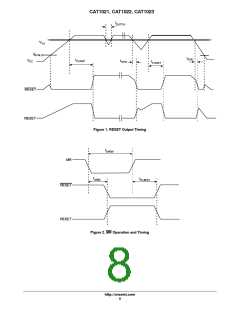
t
t
t
F
HIGH
R
t
t
LOW
LOW
SCL
t
t
HD:DAT
SU:STA
t
t
t
t
HD:STA
SU:DAT
SU:STO
SDA IN
BUF
t
AA
t
DH
SDA OUT
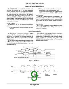
Figure 3. Bus Timing
SCL
SDA
BYTE n
t
WR
STOP
CONDITION
START
CONDITION
ADDRESS
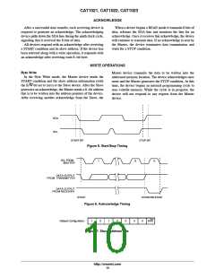
Figure 4. Write Cycle Timing
http://onsemi.com
9

 ONSEMI [ ONSEMI ]