CAT1021, CAT1022, CAT1023
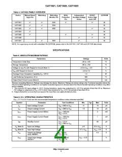
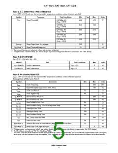
Table 6. D.C. OPERATING CHARACTERISTICS
V
CC
= 2.7 V to 5.5 V and over the recommended temperature conditions unless otherwise specified.
Symbol
Parameter
Reset Threshold
Test Conditions
Min
Typ
Max
Units
V
TH
CAT102x−45
4.50
4.75
V
(V = 5.0 V)
CC
CAT102x−42
CC
4.25
3.00
2.85
2.55
4.50
3.15
3.00
2.70
(V = 5.0 V)
CAT102x−30
(V = 3.3 V)
CC
CAT102x−28
(V = 3.3 V)
CC
CAT102x−25
(V = 3.0 V)
CC
V
Reset Output Valid V Voltage
1.00
15
V
RVALID
CC
V
(Note 4)
Reset Threshold Hysteresis
mV
RT
3. V min and V max are reference values only and are not tested.
IL
IH
4. This parameter is tested initially and after a design or process change that affects the parameter. Not 100% tested.
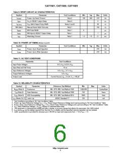
Table 7. CAPACITANCE
T = 25°C, f = 1.0 MHz, V = 5 V
A
CC
Symbol
(Note 5)
Test
Test Conditions
= 0 V
OUT
Max
8
Units
pF
C
Output Capacitance
Input Capacitance
V
V
OUT
C
(Note 5)
= 0 V
IN
6
pF
IN
Table 8. AC CHARACTERISTICS
V
CC
= 2.7 V to 5.5 V and over the recommended temperature conditions, unless otherwise specified.
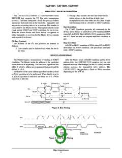
Memory Read & Write Cycle (Note 6)
Symbol
Parameter
Min
Max
400
100
Units
kHz
ns
f
Clock Frequency
SCL
t
SP
Input Filter Spike Suppression (SDA, SCL)
Clock Low Period
t
1.3
0.6
ms
LOW
t
Clock High Period
ms
HIGH
t
(Note 5)
SDA and SCL Rise Time
300
300
ns
R
t (Note 5)
SDA and SCL Fall Time
ns
F
t
Start Condition Hold Time
0.6
0.6
0
ms
HD; STA
t
Start Condition Setup Time (for a Repeated Start)
Data Input Hold Time
ms
SU; STA
HD; DAT
t
ns
t
Data Input Setup Time
100
0.6
ns
SU; DAT
SU; STO
t
Stop Condition Setup Time
ms
t
SCL Low to Data Out Valid
900
5
ns
AA
t
Data Out Hold Time
50
ns
DH
t
(Note 5)
(Note 7)
Time the Bus must be Free Before a New Transmission Can Start
Write Cycle Time (Byte or Page)
1.3
ms
BUF
t
ms
WC
5. This parameter is characterized initially and after a design or process change that affects the parameter. Not 100% tested.
6. Test Conditions according to “AC Test Conditions” table.
7. The write cycle time is the time from a valid stop condition of a write sequence to the end of the internal program/erase cycle. During the
write cycle, the bus interface circuits are disabled, SDA is allowed to remain high and the device does not respond to its slave address.
http://onsemi.com
5

 ONSEMI [ ONSEMI ]