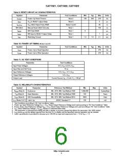
CAT1021, CAT1022, CAT1023
ACKNOWLEDGE
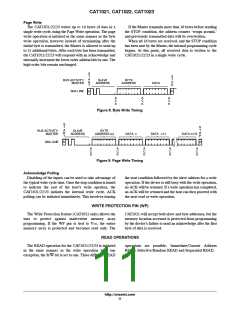
After a successful data transfer, each receiving device is
When a device begins a READ mode it transmits 8 bits of
data, releases the SDA line and monitors the line for an
acknowledge. Once it receives this acknowledge, the device
will continue to transmit data. If no acknowledge is sent by
the Master, the device terminates data transmission and
waits for a STOP condition.
required to generate an acknowledge. The acknowledging
device pulls down the SDA line during the ninth clock cycle,
signaling that it received the 8 bits of data.
All devices respond with an acknowledge after receiving
a START condition and its slave address. If the device has
been selected along with a write operation, it responds with
an acknowledge after receiving each 8−bit byte.
WRITE OPERATIONS
Byte Write
Master device transmits the data to be written into the
addressed memory location. The device acknowledges once
more and the Master generates the STOP condition. At this
time, the device begins an internal programming cycle to
non−volatile memory. While the cycle is in progress, the
device will not respond to any request from the Master
device.
In the Byte Write mode, the Master device sends the
START condition and the slave address information (with
the R/W bit set to zero) to the Slave device. After the Slave
generates an acknowledge, the Master sends a 8−bit address
that is to be written into the address pointers of the device.
After receiving another acknowledge from the Slave, the
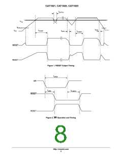
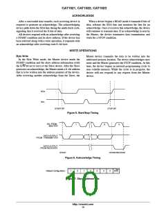
SDA
SCL
START BIT
STOP BIT
Figure 5. Start/Stop Timing
SCL FROM
MASTER
1
8
9
DATA OUTPUT
FROM TRANSMITTER
DATA OUTPUT
FROM RECEIVER
START
ACKNOWLEDGE
Figure 6. Acknowledge Timing
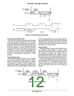
Default Configuration
1
0
1
0
0
0
0
R/W
Figure 7. Slave Address Bits
http://onsemi.com
10

 ONSEMI [ ONSEMI ]