74HC574
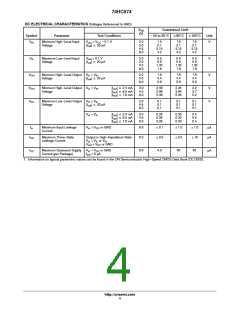
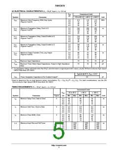
AC ELECTRICAL CHARACTERISTICS (C = 50 pF; Input t = t = 6.0 ns)
L
r
f
V
Guaranteed Limit
CC
(V)
Symbol
Parameter
*55 to 25_C v85_C v125_C
Unit
f
Maximum Clock Frequency (50% Duty Cycle)
(Figures 3 and 6)
2.0
3.0
4.5
6.0
6.0
15
30
35
4.8
10
24
28
4.0
8.0
20
MHz
max
24
t
t
t
,
Maximum Propagation Delay, Clock to Q
(Figures 3 and 6)
2.0
3.0
4.5
6.0
160
105
32
200
145
40
240
190
48
ns
ns
ns
ns
PLH
t
PHL
27
34
41
,
Maximum Propagation Delay, Output Enable to Q
(Figures 4 and 7)
2.0
3.0
4.5
6.0
150
100
30
190
125
38
225
150
45
PLZ
t
PHZ
26
33
38
,
Maximum Propagation Delay, Output Enable to Q
(Figures 4 and 7)
2.0
3.0
4.5
6 0
140
90
28
24
175
120
35
210
140
42
PZL
t
PZH
30
36
t
,
Maximum Output Transition Time, any Output
(Figures 3 and 6)
2.0
3.0
4.5
6.0
60
27
12
10
75
32
15
13
90
36
18
15
TLH
t
THL
C
Maximum Input Capacitance
10
15
10
15
10
15
pF
pF
in
C
out
Maximum Three−State Output Capacitance, Output in High−Impedance
State
8. For propagation delays with loads other than 50 pF, and information on typical parametric values, see the ON Semiconductor High−Speed
CMOS Data Book (DL129/D).
Typical @ 25°C, V = 5.0 V
CC
C
PD
Power Dissipation Capacitance (Per Enabled Output)*
24
pF
2
*Used to determine the no−load dynamic power consumption: P = C
V
f + I
V
. For load considerations, see the ON
D
PD CC
CC CC
Semiconductor High−Speed CMOS Data Book (DL129/D).
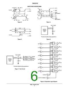
TIMING REQUIREMENTS (C = 50 pF; Input t = t = 6.0 ns)
L
r
f
Guaranteed Limit
V
– 55 to 25_C
v 85_C
v 125_C
CC
Symbol
Parameter
Figure
(V)
Min
Max
Min
Max
Min
Max
Unit
t
Minimum Setup Time, Data to Clock
5
2.0
3.0
4.6
6.0
50
40
10
9.0
65
50
13
11
75
60
15
13
ns
su
t
Minimum Hold Time, Clock to Data
Minimum Pulse Width, Clock
5
3
3
2.0
3.0
4.5
6.0
5.0
5.0
5.0
5.0
5.0
5.0
5.0
5.0
5.0
5.0
5.0
5.0
ns
ns
ns
h
t
2.0
3.0
4.5
6.0
75
60
15
13
95
80
19
16
110
90
22
19
w
t , t
r
Maximum Input Rise and Fall Times
2.0
3.0
4.5
6.0
1000
800
500
400
1000
800
500
400
1000
800
500
400
f
http://onsemi.com
5

 ONSEMI [ ONSEMI ]