74HC574
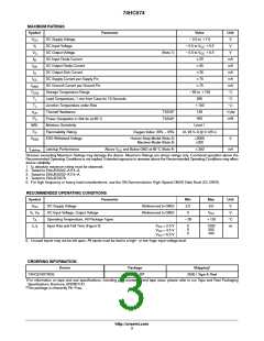
MAXIMUM RATINGS
Symbol
Parameter
Value
Unit
V
V
DC Supply Voltage
*0.5 to )7.0
CC
V
DC Input Voltage
*0.5 to V )0.5
V
I
O
CC
V
DC Output Voltage
(Note 1)
*0.5 to V )0.5
V
CC
I
DC Input Diode Current
DC Output Diode Current
DC Output Sink Current
DC Supply Current per Supply Pin
DC Ground Current per Ground Pin
Storage Temperature Range
$20
mA
mA
mA
mA
mA
_C
IK
I
$35
OK
I
$35
O
I
$75
CC
I
$75
GND
T
*65 to )150
STG
T
Lead Temperature, 1 mm from Case for 10 Seconds
Junction Temperature under Bias
Thermal Resistance
260
_C
L
T
)150
_C
_C/W
mW
J
q
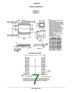
TSSOP
TSSOP
128
450
JA
P
Power Dissipation in Still Air at 85_C
Moisture Sensitivity
D
MSL
Level 1
F
Flammability Rating
Oxygen Index: 30% − 35%
UL 94 V−0 @ 0.125 in
R
V
ESD Withstand Voltage
Human Body Model (Note 2)
Machine Model (Note 3)
>2000
>200
V
ESD
I
Latchup Performance
Above V and Below GND at 85_C (Note 4)
$300
mA
Latchup
CC
Stresses exceeding Maximum Ratings may damage the device. Maximum Ratings are stress ratings only. Functional operation above the
Recommended Operating Conditions is not implied. Extended exposure to stresses above the Recommended Operating Conditions may affect
device reliability.
1. I absolute maximum rating must be observed.
O
2. Tested to EIA/JESD22−A114−A.
3. Tested to EIA/JESD22−A115−A.
4. Tested to EIA/JESD78.
5. For high frequency or heavy load considerations, see the ON Semiconductor High−Speed CMOS Data Book (DL129/D).
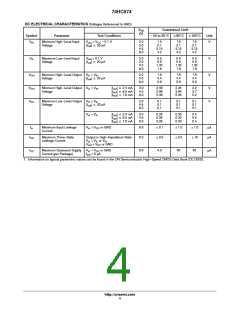
RECOMMENDED OPERATING CONDITIONS
Symbol
Parameter
Min
2.0
0
Max
Unit
V
V
DC Supply Voltage
(Referenced to GND)
(Referenced to GND)
6.0
CC
V , V
DC Input Voltage, Output Voltage
V
CC
V
I
O
T
Operating Temperature, All Package Types
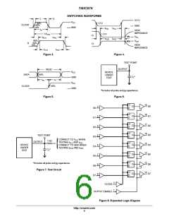
Input Rise and Fall Time (Figure 3)
*55
)125
_C
ns
A
t , t
r
V
V
V
= 2.0 V
= 4.5 V
= 6.0 V
0
0
0
1000
500
400
f
CC
CC
CC
6. Unused inputs may not be left open. All inputs must be tied to a high− or low−logic input voltage level.
ORDERING INFORMATION
†
Device
Package
Shipping
74HC574DTR2G
TSSOP−20*
2500 / Tape & Reel
†For information on tape and reel specifications, including part orientation and tape sizes, please refer to our Tape and Reel Packaging
Specifications Brochure, BRD8011/D.
*This package is inherently Pb−Free.
http://onsemi.com
3

 ONSEMI [ ONSEMI ]