AMIS-52150 Low-Power Transceiver with Clock and Data Recovery
Data Sheet
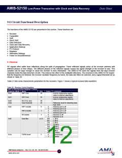
Table 21: RF Input Electrical Characteristics
Specificatio
n
Input
Settings
Conditions
Typ.
Max.
Units
KΩ
Comments
2
Resistance
Input
Capacitance
Sensitivity
Frequency
Max Input
IP3
Trim 0x00
Trim 0xff
Min. tune
Max. tune
1 Kbps
3
6
pFarads
pFarads
dBm
MHz
dBm
-117
403.5
w/CDR
Target frequency
-10
+8
dBm
IP2
+66
dBm
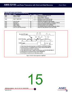
Figure 7: Received Waveform
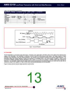
9.2 Transmitter
The RF transmitter is a non-linear open drain device. It requires a DC signal path to RFPWR, which is the output of the internal power
supply to the transmitter. The transmitter is switched on and off with the serial transmit data stream. The output requires a tuned
resonant circuit externally to form the desired waveform. This resonant circuit should be resonant at the desired output frequency. The
transmitter output also requires filtering to reduce the harmonics to acceptable levels. The circuit includes a parallel LC tank (Lp and
Cp) tuned to 402MHz (including internal capacitance) and a series LC (Ls and Cs) to produce a 403MHz output while reducing the
harmonics. The transmitter requires that the output power level be programmed, the transmit frequency be tuned and the data rate be
selected as shown in the registers of Table 23 lists some characteristic parameters for the transmitter.
Figure 8 shows what the transmit output waveform could look like.
AMI Semiconductor – Rev 4.0, Oct. 06 – M-20535-004
13
www.amis.com

 ONSEMI [ ONSEMI ]