AMIS-52150 Low-Power Transceiver with Clock and Data Recovery
Data Sheet
Table 22: Transmitter Control Registers
TX/RX Definition Control Registers
Register (HEX)
0x02
0x04
Name
Bits
All
All
4
States Comments
TX power
TX XTAL trim
TX enable
0x0c
0
Transmitter is off
1
Transmitter is on
1.1kHz
2.3kHz
5.2kHz
10.4kHz
1.18kHz
2.57kHz
7.0kHz
0x0f
Data filter
4,5,6
000
001
010
011
100
101
110
111
0
20.45kHz
Normal levels
Inverted
0x1e
TX/RX invert
5
1
Table 23: Output Impedance Characteristics
Specification
Output
Impedance
Output Power
Settings
Conditions
Resistance
Capacitance
Min.
Typ.
22
3
-26
12
-35
Max.
Units
Ω
pFarads
dBm
dBm
dBm
MHz
MHz
MHz
RFPWR 0x00
RFPWR 0xff
11
13
Harmonics
Frequency
Range
Ext circuit
Target
Quick Start
Full range
402
350
300
405
448
768
Modulation
On/Off Ratio
ASK/OOK
70
TX output
dBm
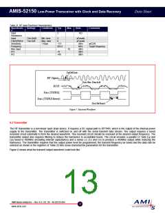
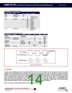
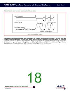
Figure 8: Transmit Waveforms
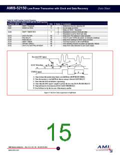
9.3 Sniff Mode
Very low power applications will want to program the AMIS-52150 to use the Sniff Mode. This mode turns the receiver and crystal
oscillator off for a programmed time. At the end of this time the receiver wakes and “sniffs” for incoming RF energy. If energy is
detected, the receiver wakes the full receive function and starts data recovery from the RF carrier. If energy is not detected, the receiver
returns to the low power or “sleep” state. The operation of the Sniff Mode is very programmable. The time that the receiver is asleep
can be programmed from microsecond to seconds. Once the receiver wakes to detect RF energy, there is a programmable delay
before the receiver checks for energy. There is another delay that accounts for circuit delays. Finally, there is a programmable delay
after energy is detected and before the receiver samples the recovered energy to determine the logical state of the recovered data.
Table 24 lists these registers. Refer to the AMIS application note “Sniff Mode” for more information.
Figure 9 and Figure 10 show waveforms that show the timing of the Sniff Mode.
AMI Semiconductor – Rev 4.0, Oct. 06 – M-20535-004
14
www.amis.com

 ONSEMI [ ONSEMI ]