AMIS-52150 Low-Power Transceiver with Clock and Data Recovery
Data Sheet
8.6 GND, Ground
The GND pin is the ground connection for the digital and analog circuits in the AMIS-52150.
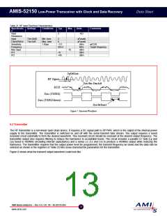
8.7 CLKOUT, Internal Clock Output
The CLKOUT pin is an output for the RC oscillator, crystal oscillator signal or the recovered data clock. The crystal oscillator signal
output can be divided by 2, 3 or 4. The pin can also be programmed to output the signal from the recovered data clock function. For
more information about the clock and data recovery (CDR) function of the AMIS-52150, refer to the section of this document on clock
and data recovery.
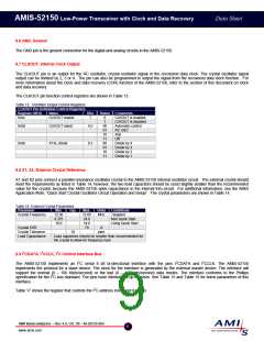
The CLKOUT pin function control registers are shown in Table 13.
Table 13: Oscillator Output Control Registers
CLKOUT Pin Definition Control Registers
Register (HEX)
Name
Bits
States Comments
0x0c
CLKOUT enable
7
0
CLKOUT is enabled
1
CLKOUT is disabled
Automatic control
RC OSC
Xtal
Off
Divide by 4
Divide by 3
Divide by 2
Divide by 1
0x0d
0x0e
CLKOUT select
XTAL divide
4,5
0,1
00
01
10
11
00
01
10
11
8.8 X1, X2, External Crystal Reference
X1 and X2 pins connect a parallel resonance oscillator crystal to the AMIS-52150 internal oscillator circuit. The external crystal should
meet the requirements as listed in Table 14, however, the two load capacitors should be sized slightly smaller than the recommended
value for the crystal, because the AMIS-52150 adds capacitance in the internal trim circuit. For additional information, see the AMIS
Application Note; “Quick Start Crystal Oscillator Circuit Operation and Setup”. The crystal parameters are shown in Table 14.
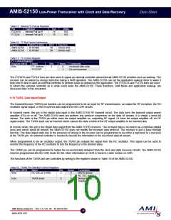
Table 14: External Crystal Parameters
Parameter
Crystal Frequency
Min.
12.56
9.375
10.9
Typ.
Max.
12.65
24.0
14.0
70
Units
MHz
Conditions
Targeted
Non Quick Start
Using Quick Start
Crystal ESR
Ω
Crystal Tolerance
Load Capacitance
10
ppm
Load capacitors should be smaller than recommended for
the crystal to allow for frequency tune
8.9 I2CDATA, I2CCLK, I2C Control Interface Bus
The AMIS-52150 implements an I2C serial 8 bit bi-directional interface with the pins I2CDATA and I2CCLK. The AMIS-52150
implements the protocol for a slave device. The clock for the interface is generated by the external master device. The interface will
support the normal (0 – 100 Kbits/second) or the fast (0 – 400Kbits/second) data modes. The interface conforms to the Phillips
specification for the I2C bus standard. The pins have internal pull up resistors. See Table 15 and Table 16 for some parameters of this
interface.
Table 17 shows the register that controls the I2C address increment function.
AMI Semiconductor – Rev 4.0, Oct. 06 – M-20535-004
9
www.amis.com

 ONSEMI [ ONSEMI ]