TDA8950
NXP Semiconductors
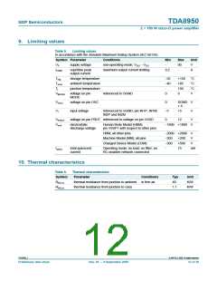
2 × 150 W class-D power amplifier
8.2 Pulse width modulation frequency
The output signal of the amplifier is a PWM signal with a carrier frequency that typically
lies between 300 kHz and 400 kHz. Using a 2nd-order LC demodulation filter in the
application results in an analog audio signal across the loudspeaker. The carrier
frequency is determined by an external resistor ROSC, connected between pin OSC and
pin VSSA. An optimal setting for the carrier frequency is between 300 kHz and 400 kHz.
Using an external resistor of 30 kΩ on pin OSC, the carrier frequency is set to 345 kHz.
For more details see Table 8.
If two or more class-D amplifiers are used in the same audio application, it is
recommended that all devices operate at the same switching frequency by using an
external clock circuit.
Due to an internal clock divider:
• The external applied clock frequency must have the double frequency of the output
PWM frequency.
• The duty cycle of the external clock is not critical for product performance.
8.3 Protections
The following protections are included in TDA8950:
• Thermal protections:
– Thermal FoldBack (TFB)
– OverTemperature Protection (OTP)
• OverCurrent Protection (OCP, diagnostic via pin PROT)
• Window Protection (WP)
• Supply voltage protections:
– UnderVoltage Protection (UVP)
– OverVoltage Protection (OVP)
– UnBalance Protection (UBP)
The reaction of the device to the different fault conditions differs per protection.
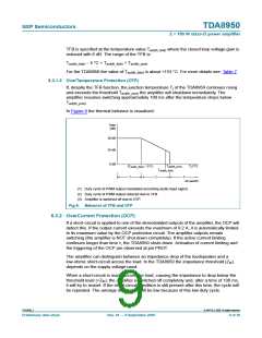
8.3.1 Thermal protection
In the TDA8950 an advanced thermal protection strategy is implemented. It consists of a
TFB function that gradually reduces the out put power within a certain temperature range.
When temperature is still rising an OTP is implemented which shuts down the device
completely.
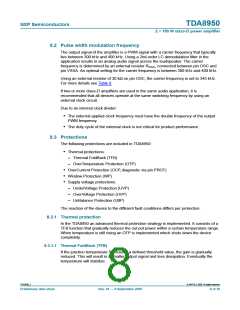
8.3.1.1 Thermal FoldBack (TFB)
If the junction temperature Tj exceeds a defined threshold value, the gain is gradually
reduced. This will result in a smaller output signal and less dissipation. Eventually the
temperature will stabilize.
TDA8950_1
© NXP B.V. 2008. All rights reserved.
Preliminary data sheet
Rev. 01 — 9 September 2008
8 of 39

 NXP [ NXP ]