TDA8950
NXP Semiconductors
2 × 150 W class-D power amplifier
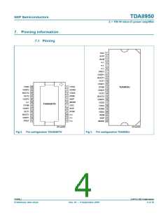
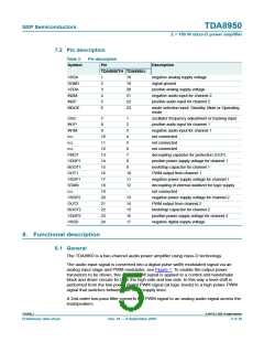
7.2 Pin description
Table 3.
Symbol
Pin description
Pin
Description
TDA8950TH TDA8950J
VSSA
SGND
VDDA
IN2M
1
2
3
4
5
6
18
19
20
21
22
23
negative analog supply voltage
signal ground
positive analog supply voltage
negative audio input for channel 2
positive audio input for channel 2
IN2P
MODE
mode selection input: Standby, Mute or Operating
mode
OSC
7
1
oscillator frequency adjustment or tracking input
positive audio input for channel 1
negative audio input for channel 1
not connected
IN1P
8
2
IN1M
n.c.
9
3
10
11
12
13
14
15
16
17
18
19
20
21
22
23
24
4
n.c.
5
not connected
n.c.
6
not connected
PROT
VDDP1
BOOT1
OUT1
VSSP1
STABI
n.c.
7
decoupling capacitor for protection (OCP)
positive power supply voltage for channel 1
bootstrap capacitor for channel 1
PWM output from channel 1
8
9
10
11
12
-
negative power supply voltage for channel 1
decoupling of internal stabilizer for logic supply
not connected
VSSP2
OUT2
BOOT2
VDDP2
VSSD
13
14
15
16
17
negative power supply voltage for channel 2
PWM output from channel 2
bootstrap capacitor for channel 2
positive power supply voltage for channel 2
negative digital supply voltage
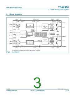
8. Functional description
8.1 General
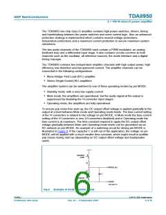
The TDA8950 is a two-channel audio power amplifier using class-D technology.
The audio input signal is converted into a digital pulse width modulated signal via an
analog input stage and PWM modulator, see Figure 1. To enable the output power
transistors to be driven, this digital PWM signal is applied to a control and handshake
block and driver circuits for both the high side and low side. In this way a level shift is
performed from the low power digital PWM signal (at logic levels) to a high power PWM
signal that switches between the main supply lines.
A 2nd-order low-pass filter converts the PWM signal to an analog audio signal across the
loudspeakers.
TDA8950_1
© NXP B.V. 2008. All rights reserved.
Preliminary data sheet
Rev. 01 — 9 September 2008
5 of 39

 NXP [ NXP ]