TDA8950
NXP Semiconductors
2 × 150 W class-D power amplifier
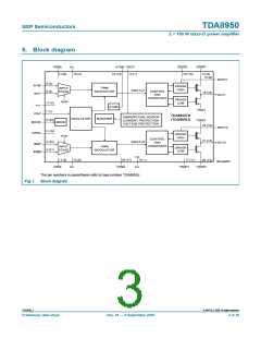
The TDA8950 one-chip class-D amplifier contains high power switches, drivers, timing
and handshaking between the power switches and some control logic. Also an advanced
protection strategy is implemented which contains several voltage protections,
temperature protections and a maximum current protection to secure maximum system
robustness.
The two audio channels of the TDA8950 each contain a PWM modulator, an analog
feedback loop and a differential input stage. It also contains circuits common to both
channels such as the oscillator, all reference sources, the mode interface and a digital
timing manager.
The TDA8950 contains two independent amplifier channels with high output power, high
efficiency, low distortion and low quiescent current. The amplifier channels can be
connected in the following configurations:
• Mono Bridge-Tied Load (BTL) amplifier
• Stereo Single-Ended (SE) amplifiers
The amplifier system can be switched to one of three operating modes by pin MODE:
• Standby mode; with a very low supply current
• Mute mode; the amplifiers are operational, but the audio signal at the output is
suppressed by disabling the VI-converter input stages
• Operating mode; the amplifiers are fully operational
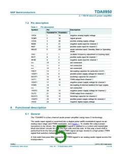
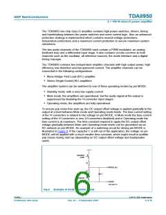
To ensure pop noise-free start-up, the DC output offset voltage is applied gradually to the
output at a level between Mute mode and Operating mode levels. The bias current setting
of the VI converters is related to the voltage on pin MODE; in Mute mode the bias current
setting of the VI converters is zero (VI converters disabled) and in Operating mode the
bias current is at maximum. The time constant required to apply the DC output offset
voltage gradually between Mute and Operating mode levels can be generated via an
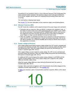
RC-network on pin MODE. An example of a switching circuit for driving pin MODE is
illustrated in Figure 4. If the capacitor C is left out of the application, the voltage on pin
MODE will be applied with a much smaller time-constant, which might result in audible
pop noises during start-up (depending on DC output offset voltage and loudspeaker
used).
+
5 V
standby/
mute
R
MODE pin
R
C
mute/on
SGND
001aab172
Fig 4. Example of mode selection circuit
Rev. 01 — 9 September 2008
TDA8950_1
© NXP B.V. 2008. All rights reserved.
Preliminary data sheet
6 of 39

 NXP [ NXP ]