TDA8950
NXP Semiconductors
2 × 150 W class-D power amplifier
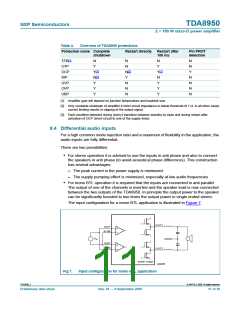
Table 4.
Overview of TDA8950 protections
Protection name Complete
shutdown
Restart directly Restart after
Pin PROT
detection
100 ms
TFB[1]
OTP
OCP
WP
N
N
N
N
N
Y
N
N
N
N
Y
N
N[2]
Y
Y[2]
Y[2]
N[3]
Y
Y
N
UVP
OVP
UBP
N
Y
Y
N
Y
Y
N
Y
[1] Amplifier gain will depend on junction temperature and heatsink size.
[2] Only complete shutdown of amplifier if short-circuit impedance is below threshold of 1 Ω. In all other cases
current limiting results in clipping of the output signal.
[3] Fault condition detected during (every) transition between standby-to-mute and during restart after
activation of OCP (short-circuit to one of the supply lines).
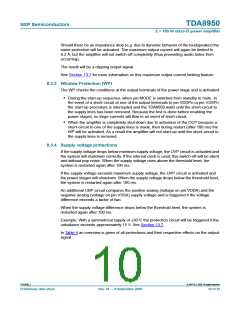
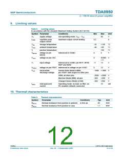
8.4 Differential audio inputs
For a high common mode rejection ratio and a maximum of flexibility in the application, the
audio inputs are fully differential.
There are two possibilities:
• For stereo operation it is advised to use the inputs in anti phase and also to connect
the speakers in anti phase (to avoid acoustical phase differences). This construction
has several advantages:
– The peak current in the power supply is minimized
– The supply pumping effect is minimized, especially at low audio frequencies
• For mono BTL operation it is required that the inputs are connected in anti parallel.
The output of one of the channels is inverted and the speaker load is now connected
between the two outputs of the TDA8950. In principle the output power to the speaker
can be significantly boosted to two times the output power in single ended stereo.
The input configuration for a mono BTL application is illustrated in Figure 7.
OUT1
IN1P
IN1M
V
SGND
in
IN2P
IN2M
OUT2
power stage
mbl466
Fig 7.
Input configuration for mono BTL application
Rev. 01 — 9 September 2008
TDA8950_1
© NXP B.V. 2008. All rights reserved.
Preliminary data sheet
11 of 39

 NXP [ NXP ]