TDA8950
NXP Semiconductors
2 × 150 W class-D power amplifier
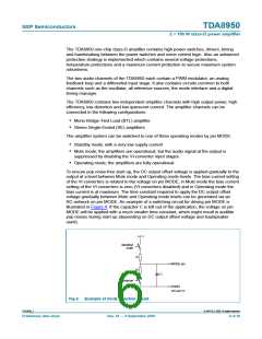
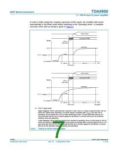
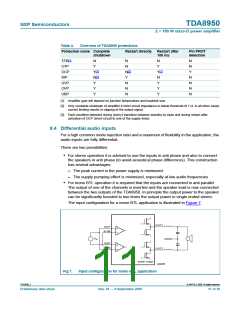
In order to fully charge the coupling capacitors at the inputs, the amplifier will remain
automatically in the Mute mode before switching to the Operating mode. A complete
overview of the start-up timing is given in Figure 5.
audio output
(1)
modulated PWM
V
MODE
50 %
duty cycle
operating
> 4.2 V
mute
2.2 V < V
< 3 V
MODE
standby
0 V (SGND)
time
100 ms
> 350 ms
50 ms
audio output
(1)
modulated PWM
V
MODE
50 %
duty cycle
operating
> 4.2 V
mute
2.2 V < V
< 3 V
MODE
standby
0 V (SGND)
time
100 ms
> 350 ms
50 ms
001aah657
(1) First 1⁄4 pulse down.
Upper diagram: When switching from standby to mute, there is a delay of approximately 100 ms
before the output starts switching. The audio signal is available after VMODE has been set to
operating, but not earlier than 150 ms after switching to mute. For pop noise-free start-up it is
recommended that the time constant applied to pin MODE is at least 350 ms for the transition
between mute and operating.
Lower diagram: When switching directly from standby to operating, there is a first delay of 100 ms
before the outputs starts switching. The audio signal is available after a second delay of 50 ms. For
pop noise-free start-up it is recommended that the time constant applied to pin MODE is at least
500 ms for the transition between standby and operating.
Fig 5. Timing on mode selection input
TDA8950_1
© NXP B.V. 2008. All rights reserved.
Preliminary data sheet
Rev. 01 — 9 September 2008
7 of 39

 NXP [ NXP ]