Philips Semiconductors
Product specification
Economy Autosync Deflection Controller
(EASDC)
TDA4858
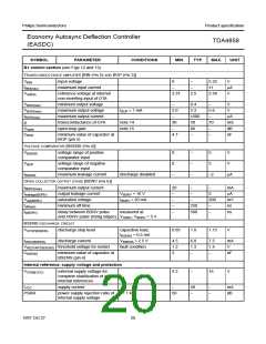
SYMBOL
PARAMETER
CONDITIONS
MIN.
TYP.
MAX.
UNIT
PLL2 phase detector [HFLB (pin 1) and HPLL2 (pin 31)]
∆φPLL2
PLL2 control (advance of
horizontal drive with respect to
middle of horizontal flyback)
maximum advance
minimum advance
36
−
−
−
%
−
7
%
td(HFLB)
delay between middle of
horizontal sync and middle of
horizontal flyback
HPOS (pin 30) grounded
−
200
−
ns
VPROT(HPLL2)
Icharge(HPLL2)
maximum voltage for PLL2
protection mode/soft start
−
−
4.4
15
−
−
V
charge current for external
capacitor during soft start
V
HPLL2 < 3.7 V
µA
HORIZONTAL FLYBACK INPUT [HFLB (PIN 1)]
VHFLB
positive clamping level
negative clamping level
positive clamping current
negative clamping current
slicing level
IHFLB = 5 mA
HFLB = −1 mA
−
−
−
−
−
5.5
−0.75
−
−
−
6
V
I
V
IHFLB
mA
mA
V
−
−2
VHFLB
2.8
−
Output stage for line driver pulses [HDRV (pin 7)]
OPEN COLLECTOR OUTPUT STAGE
VHDRV
saturation voltage
IHDRV = 20 mA
HDRV = 60 mA
−
−
−
−
−
−
0.3
0.8
10
V
I
V
Ileakage(HDRV)
output leakage current
VHDRV = 16 V
µA
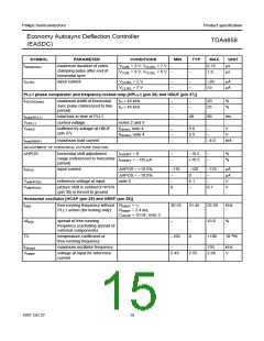
AUTOMATIC VARIATION OF DUTY FACTOR
tHDRV(OFF)/tH
relative tOFF time of HDRV
output; measured at
HDRV = 3 V; HDRV duty factor
is determined by the relation
IHREF/IVREF
IHDRV = 20 mA;
fH = 31.45 kHz; see Fig.9
42
45
48
%
%
%
V
I
HDRV = 20 mA;
fH = 57 kHz; see Fig.9
HDRV = 20 mA;
fH = 90 kHz; see Fig.9
45
46.3
48
47.7
49.4
I
46.6
X-ray protection [XRAY (pin 2)]
VXRAY
slicing voltage level
6.14
10
500
−
6.38
−
6.64
V
tW(XRAY)
RI(XRAY)
minimum width of trigger pulse
−
−
−
−
µs
kΩ
kΩ
V
input resistance at XRAY
(pin 2)
V
V
XRAY < 6.38 V + VBE
XRAY > 6.38 V + VBE
−
5
VRESET(VCC)
supply voltage for reset of
X-ray latch
−
5.6
1997 Oct 27
16

 NXP [ NXP ]