Philips Semiconductors
Product specification
Economy Autosync Deflection Controller
(EASDC)
TDA4858
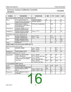
SYMBOL
PARAMETER
CONDITIONS
MIN.
TYP.
MAX.
UNIT
B+ control section (see Figs 12 and 13)
TRANSCONDUCTANCE AMPLIFIER [BIN (PIN 5) AND BOP (PIN 3)]
VBIN
input voltage
0
−
−
5.25
V
IBIN(max)
Vref(int)
maximum input current
−
±1
µA
reference voltage at internal
non-inverting input of OTA
2.37
2.5
2.58
V
VBOP(min)
VBOP(max)
IBOP(max)
g
minimum output voltage
maximum output voltage
maximum output current
transconductance of OTA
open-loop gain
−
0.4
5.3
±500
50
−
V
I
BOP < 1 mA
5.0
−
5.6
−
V
µA
mS
dB
nF
note 14
note 15
30
−
70
−
Gopen
86
CBOP
minimum value of capacitor at
BOP (pin 3)
4.7
−
−
VOLTAGE COMPARATOR [BSENS (PIN 4)]
VBSENS
voltage range of positive
comparator input
0
0
−
−
−
−
5
V
VBOP
voltage range of negative
comparator input
5
V
IBSENS
maximum leakage current
discharge disabled
VBDRV = 16 V
−2
µA
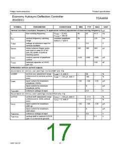
OPEN COLLECTOR OUTPUT STAGE [BDRV (PIN 6)]
IBDRV(max)
Ileakage(BDRV)
Vsat(BDRV)
toff(min)
maximum output current
output leakage current
saturation voltage
20
−
−
−
mA
µA
mV
ns
−
3
IBDRV < 20 mA
−
−
300
−
minimum off-time
−
250
500
td(BDRV)
delay between BDRV pulse
measured at
−
−
ns
and HDRV pulse (rising edges) VHDRV, VBDRV = 3 V
BSENS DISCHARGE CIRCUIT
VSTOP(BSENS)
discharge stop level
capacitive load;
IBSENS = 0.5 mA
0.85
1.0
1.15
V
IDISC(BSENS)
discharge current
V
BSENS > 2.5 V
4.5
1.2
2
6.0
1.3
−
7.5
1.4
−
mA
V
VRESTART(BSENS) threshold voltage for restart
fault condition
CBSENS
minimum value of capacitor at
BSENS (pin 4)
nF
Internal reference, supply voltage and protection
VSTAB(VCC)
external supply voltage for
complete stabilization of all
internal references
9.2
−
16
V
IVCC
supply current
−
49
−
−
mA
dB
PSRR
power supply rejection ratio of f = 1 kHz
internal supply voltage
50
−
1997 Oct 27
20

 NXP [ NXP ]