LPC546xx
NXP Semiconductors
32-bit ARM Cortex-M4 microcontroller
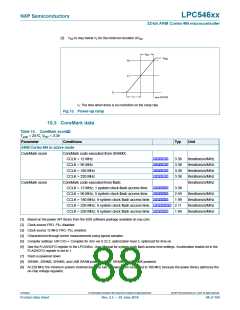
[3] VDD to stay below V2 for the minimum duration of twd
.
t
wd
V
DD
V
V
2
1
0
t
1
aaa-025788
t1: The time when there is no restriction on the ramp rate.
Fig 13. Power-up ramp
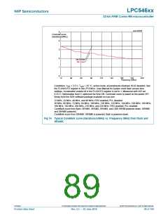
10.3 CoreMark data
Table 14. CoreMark score[1]
Tamb = 25C, VDD = 3.3V
Parameter
Conditions
Typ
Unit
ARM Cortex-M4 in active mode
CoreMark score
CoreMark code executed from SRAMX;
[2][4][5][7][8]
[2][4][5][7][8]
[3][4][5][7][8]
[3][4][5][7][8]
CCLK = 12 MHz
3.38
3.38
3.38
3.38
Iterations/s/MHz
Iterations/s/MHz
Iterations/s/MHz
Iterations/s/MHz
Iterations/s/MHz
CCLK = 96 MHz
CCLK = 180 MHz
CCLK = 220 MHz
CoreMark score
CoreMark code executed from flash;
CCLK = 12 MHz; 1 system clock flash access time.
CCLK = 96 MHz; 5 system clock flash access time.
CCLK = 180 MHz; 9 system clock flash access time.
CCLK = 220 MHz; 8 system clock flash access time.
CCLK = 220 MHz; 9 system clock flash access time.
[2][4][5][6][8]
[2][4][5][6][8]
[3][4][5][6][8]
[3][4][5][6][8][9]
[3][4][5][6][8]
3.38
2.59
1.99
2.11
1.99
Iterations/s/MHz
Iterations/s/MHz
Iterations/s/MHz
Iterations/s/MHz
[1] Based on the power API library from the SDK software package available on nxp.com.
[2] Clock source FRO. PLL disabled.
[3] Clock source 12 MHz FRO. PLL enabled.
[4] Characterized through bench measurements using typical samples.
[5] Compiler settings: IAR C/C++ Compiler for Arm ver 8.22.2, optimization level 3, optimized for time on.
[6] See the FLASHCFG register in the LPC546xx. User Manual for system clock flash access time settings. Acceleration enable bit in the
FLASHCFG register is set to 1.
[7] Flash is powered down
[8] SRAM1, SRAM2, SRAM3, and USB SRAM powered down. SRAM0 and SRAMX powered.
[9] At 220 MHz the minimum system clock/access time can be lower when compared to 180 MHz because the power library optimizes the
on-chip voltage regulator.
LPC546xx
All information provided in this document is subject to legal disclaimers.
© NXP Semiconductors N.V. 2018. All rights reserved.
Product data sheet
Rev. 2.5 — 20 June 2018
88 of 169

 NXP [ NXP ]