NAND01G-B2B, NAND02G-B2C
DC and AC parameters
11
DC and AC parameters
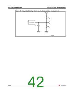
This section summarizes the operating and measurement conditions, and the DC and AC
characteristics of the device. The parameters in the DC and AC characteristics tables that
follow, are derived from tests performed under the measurement conditions summarized in
Table 20: Operating and AC measurement conditions. Designers should check that the
operating conditions in their circuit match the measurement conditions when relying on the
quoted parameters.
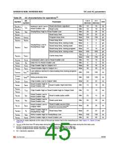
Table 20. Operating and AC measurement conditions
NAND flash
Parameter
Units
Min
Max
1.8 V devices
3 V devices
1.7
2.7
0
1.95
3.6
70
V
V
Supply voltage (VDD
)
Grade 1
°C
°C
pF
pF
V
Ambient temperature (TA)
Grade 6
–40
85
1.8 V devices
3 V devices (2.7 - 3.6 V)
1.8 V devices
3 V devices
30
50
Load capacitance (CL)
(1 TTL GATE and CL)
0
VDD
2.4
Input pulses voltages
0.4
V
Input and output timing ref. voltages
Output circuit resistor Rref
Input rise and fall times
VDD/2
8.35
5
V
kΩ
ns
(1)
Table 21. Capacitance
Symbol
Parameter
Input capacitance
Input/output capacitance(2)
Test condition
Typ
Max
Unit
CIN
VIN = 0 V
VIL = 0 V
10
10
pF
pF
CI/O
1. TA = 25 °C, f = 1 MHz. CIN and CI/O are not 100% tested.
2. Input/output capacitances double in stacked devices.
41/60

 NUMONYX [ NUMONYX B.V ]