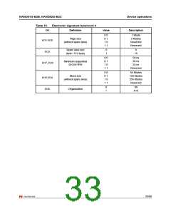
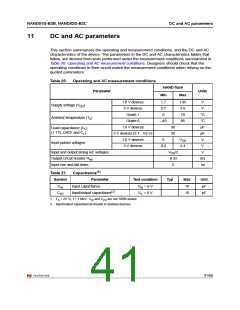
NAND01G-B2B, NAND02G-B2C
Software algorithms
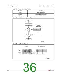
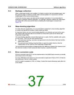
8.3
Garbage collection
When a data page needs to be modified, it is faster to write to the first available page, and
the previous page is marked as invalid. After several updates it is necessary to remove
invalid pages to free some memory space.
To free this memory space and allow further program operations it is recommended to
implement a garbage collection algorithm. In a garbage collection software the valid pages
are copied into a free area and the block containing the invalid pages is erased (see
Figure 16).
8.4
Wear-leveling algorithm
For write-intensive applications, it is recommended to implement a wear-leveling algorithm
to monitor and spread the number of write cycles per block.
In memories that do not use a wear-leveling algorithm not all blocks get used at the same
rate. Blocks with long-lived data do not endure as many write cycles as the blocks with
frequently-changed data.
The wear-leveling algorithm ensures that equal use is made of all the available write cycles
for each block. There are two wear-leveling levels:
■
First level wear-leveling, new data is programmed to the free blocks that have had the
fewest write cycles
■
Second level wear-leveling, long-lived data is copied to another block so that the
original block can be used for more frequently-changed data.
The second level wear-leveling is triggered when the difference between the maximum and
the minimum number of write cycles per block reaches a specific threshold.
8.5
Error correction code
An error correction code (ECC) can be implemented in the NAND flash memories to identify
and correct errors in the data.
For every 2048 bits in the device it is recommended to implement 22 bits of ECC (16 bits for
line parity plus 6 bits for column parity).
An ECC model is available in VHDL or Verilog. Contact the nearest Numonyx sales office for
more details.
37/60

 NUMONYX [ NUMONYX B.V ]