Maximum ratings
NAND01G-B2B, NAND02G-B2C
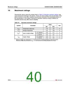
10
Maximum ratings
Stressing the device above the ratings listed in Table 19: Absolute maximum ratings, may
cause permanent damage to the device. These are stress ratings only and operation of the
device at these or any other conditions above those indicated in the operating sections of
this specification is not implied. Exposure to absolute maximum rating conditions for
extended periods may affect device reliability.
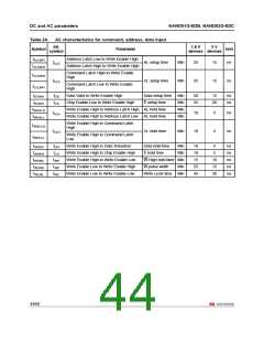
Table 19. Absolute maximum ratings
Value
Symbol
Parameter
Unit
Min
Max
TBIAS
TSTG
Temperature under bias
– 50
– 65
125
150
2.7
4.6
2.7
4.6
°C
°C
V
Storage temperature
1.8 V devices
3 V devices
1.8 V devices
3 V devices
– 0.6
– 0.6
– 0.6
– 0.6
(1)
VIO
Input or output voltage
V
V
VDD
Supply voltage
V
1. Minimum voltage may undershoot to –2 V for less than 20 ns during transitions on input and I/O pins.
Maximum voltage may overshoot to VDD + 2 V for less than 20 ns during transitions on I/O pins.
40/60

 NUMONYX [ NUMONYX B.V ]